The ARM Cortex A73 - Artemis Unveiled
by Andrei Frumusanu on May 29, 2016 11:00 PM EST- Posted in
- Mobile
- Arm
- ARMv8
- Artemis
- Cortex A73
The Cortex A73’s Microarchitecture
Before we go on to talk about the Cortex A73’s microarchitecture and how it differs to the A72 and improves on the A17, I created a diagram of the former’s pipeline structure to be able to better showcase the design from a higher level perspective.
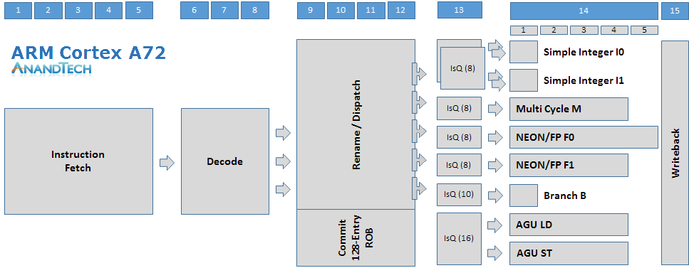
The Cortex A72 is a 15+ stage OoO-pipeline design with a 128 bit fetch and 3-wide decode stage on the instruction-side. Decoding up to 3 instructions into micro-operations (µops) these are then fed into the rename/dispatch stages. The dispatch unit can dispatch up to 5 µops per cycle that feed up to 7 issue queues which in turn schedule µops into 8 execution pipelines.
We find two simple ALUs capable of basic operations such as additions and shifting. Integer multiplication, division and multiply-accumulate operations are handled by a dedicated multi-cycle integer pipeline. Floating point as well as ASIMD and NEON operations are handled by two pipelines, some of the capabilities we’ll go into detail later on. We find a single branch monitor and two dedicated Load and Store AGUs.
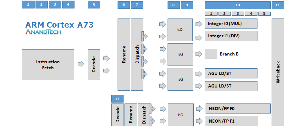
The Cortex A73 looks very similar to the Cortex A17, which in turn is quite different from ARM’s current Austin family of 3-wide decode microarchitectures. The microarchitecture has fundamentally shorter pipeline stages, mostly due to optimizations on the in-order front-end. The fetch stage is only 4 stages deep compared to the 5 stages on the A72. The decode stage is particularly an element which shortens the pipeline length as the A17’s and A73’s decoders are able to decode most instructions in a single cycle as opposed to 3 cycles on the A72. Micro-operations that feed into the floating point pipelines pass through an additional decode stage, making this an 11-12+ deep architecture depending on the type of instructions.
Compared to the A17 the A73 increases its maximum overall dispatch rate from 4 µops to 6 µops. The reservation station for the FP pipeline can still dispatch 2 µops into the common NEON issue queue, the same as on the A17, but the dispatch rate of the integer reservation station has been increased to up to 4 µops, up from 2 on the A17. The dispatch here can feed up to 2 µops for each of the 3 issue queues.
We still have two FP pipelines, and the A73 actually doesn’t change much from the A72 in terms of their capabilities as the A72 had borrowed the A73’s new design. There’s again a single branch monitor, however the AGUs, again like on the A17, are both capable of load and store operations as opposed to the dedicated units found on the A72. Finally on the integer pipelines we see the capabilities of the multi-cycle integer pipeline dissolved into two more complex ALUs. One ALU is capable of multiplication while the other one has integer divide capabilities, all on top of their basic addition and shifter duties. Multiply-accumulate is no longer dedicated and requires execution on both ALUs in tandem.
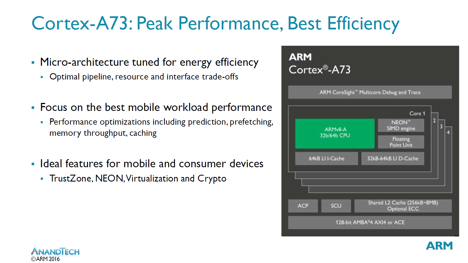
As the A73 is based off the A17 it continues that microarchitecture’s philosophy: Optimizing the pipeline, resource and interface to achieve the best possible performance at the least possible power consumption while targeting mobile workloads. ARM states that it has especially paid lots of attention to the balance between AArch32 and AArch64 ARMv8 states of the microarchitecture so to that neither is in a disadvantage in either performance or power.
At the cluster level the A73 continues ARM’s quad-core strategy so we are able to use 1 to 4 cores per cluster. The Snoop Coherency Unit (SCU) enables coherency between the cores in a cluster. The L2 cluster is configurable up to 8MB – the same as the A17 and double the amount the A72 supports. ARM still envisions that most vendors will choose to use configurations of 1 to 2MB in consumer products. The L2 cache is inclusive of the L1 cache.
The Accelerated Coherency Port (ACP) is optional and can be left out for mobile designs. The ACP is used for attaching accelerator blocks which are then coherent with the CPU cores and can also make use of the L2 cache. Traditionally this has been mainly something targeted at networking use-cases which weren't as relevant in the mobile space, however ARM sees future potential in machine-learning and computer vision where specialized accelerators can bring tangible performance benefits to a platform.
As opposed to the A15/57/72 who also targeted industrial and large-scale systems, the A73 is mainly targeting the consumer market. Consequently, it drops support the AMBA 5 Coherent Hub Interface (CHI) standard and instead only runs the AMBA 4 ACE (Accelerated Coherency Extensions) standard via a bi-directional 128bit interface. This saves on area and complexity of the microarchitecture's interface. Currently all ARM Cortex big.LITTLE SoCs use ACE interfaces to connect to coherent interconnects such as the CCI-400. Another effect of the design not targeting industrial applications is the lack of support of ECC on the L1 caches, however the L2 can be configured with the feature.

Going deeper into the microarchitecture improvements of Artemis, we start on the instruction side. The I-side on the A73 has been designed to sustain maximum throughput to the rest of the core, as this is one of the most important aspects of a microarchitecture to be able to achieve the best possible IPC. At the same time ARM had to work within set constraints to be able to maintain power consumption.
ARM calls the A17 and A73 “slot-based microarchitectures” which is related to the way the resources are handled and shared among the different blocks of the µarch. As ARM explains it, the A73 sports 8 “slots” where each slot can independently handle all resources on the instruction side. The main advantage of this is that each slot can retrieve information from previous slots in cases of small loops, and thus able to eliminate redundant access to resources on the I-side of the pipeline, a design which is optimal for power consumption. Each slot is given large resources to attain maximum performance, however ARM didn’t want to go into too much detail on this part of the µarch.
The L1 instruction cache 4-way associative and is fixed at 64KB. This is an upgrade over the 32/64KB configuration options on the A17 and also higher than the 48KB that the A72 sports. The upgrade in the L1I cache is a key aspect of the performance improvements of the A73. ARM states that it spent a lot of time optimizing the I-cache for performance and power. One example of this was the way the cache is accessed; if an access is performed but the requesting resource no longer needs the data, the access can be killed on-the-fly to be able to save power.
The instruction fetch block has been optimized to increase maximum throughput to the rest of the core. One optimization was a focus on the removal of “bubbles” for higher IPC. In previous microarchitectures even if a prediction was correct and the I-side was able to send maximum throughput to the decode stage, one could still encounter bubbles as soon as the instruction hit the decode stage it split into micro-operations which introduced them. The A73 detects such cases earlier and is able to send µops directly to the decode stage, resulting in what ARM states in an almost practical elimination of bubbles.
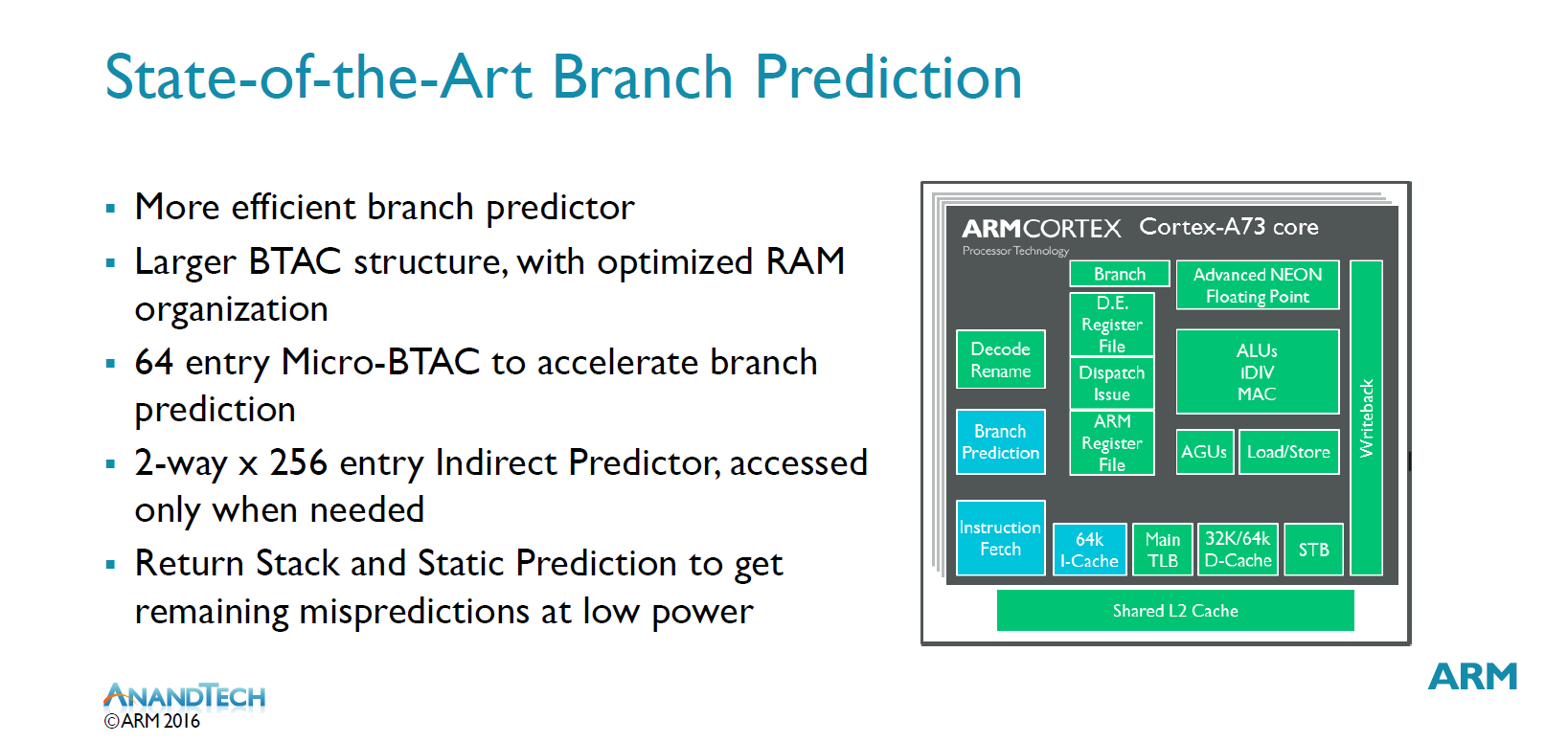
The A73 uses a new “state-of-the-art” branch predictor with very accurate branch prediction. The A73 claims to have a larger BTAC (Branch Target Address Cache) structure, however we unfortunately don’t have any concrete figures on how this has improved. We see the introduction of a new 64-entry “micro-BTAC” which is used to accelerate branch prediction. These two main units are claimed to be able to predict almost all branches.
For the remaining mispredictions the µarch disposes of a static branch predictor and a return stack which is a stack of nested subroutine return addresses. The indirect predictor seems to be an addition when compared to the A17’s branch prediction design, however it's not clear how this 2-way x 256-entry indirect predictor compares or if it differs to the one on the A72.
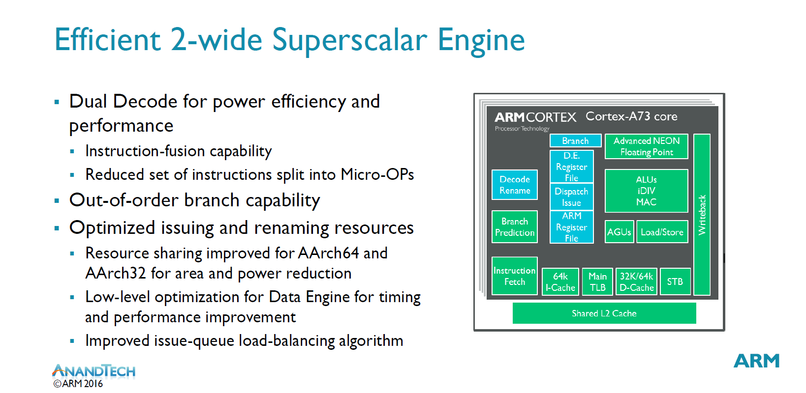
ARM is confident in its ability to increase performance of a 2-wide core while keeping or improving its efficiency. Power is only active to logic that is working on the current “set” of resources. The decoder has seen improvements in its capability to fuse instructions together. Instruction fusion for common idioms is critical for overall performance, but it’s rough to detect them. The A73 pushes further pushes its detection of such idioms through help of former events and is able to detect specific sequences with help of information alongside the whole pipeline.
Splitting instructions into more µops can be helpful for timing reasons, however it also reduces your overall IPC. The A73 reduces the set of instructions which are split into µops to be able to improve on this aspect of the decoder performance.
As mentioned earlier in the overview diagram, the decoder stage is extremely aggressive and is able to decode most instructions in just 1 cycle as opposed to the 3 cycles the A72 µarch family takes. Micro-operations feeding into the ASIMD/NEON pipelines go through an additional decode stage. ARM says that dual load/store units (as opposed to dedicated load and store units) were important to achieving this 1-2 cycle decode capability.
Dispatch rate has been improved over the A17 and now the integer part of the reservation stations can dispatch up to 4 µops into the 3 issue queues (2 µops per IQ) serving the ALUs, AGUs and branch monitor.
An important divergance from the A15/57/72 microarchitectures is the use of a physical register file instead of an architectural one. The benefits of this are a simplification around the rename stage which allow for power savings with high performance. Much like on the A17 this allows for a theoretical "unlimited OoO window", although there are still real limits to it, it does eliminate instruction window bottlenecks for some cases. ARM calls this a "major philosophical change in Out-of-Order micro-architecture approach".
The A73 focuses on optimizing resources from the rename stage up to the issue-queues. The OoO policies on which the issue-queues run on can have a large impact on performance, so special care has been taken to dispatch to the most effective issue-queue. Arbitration in the queues can change on the fly depending on various events, for example when it’s detected that you are in a stream it’s better to issue all store operations in order to be able to deal with a full cache line when feeding the memory system.
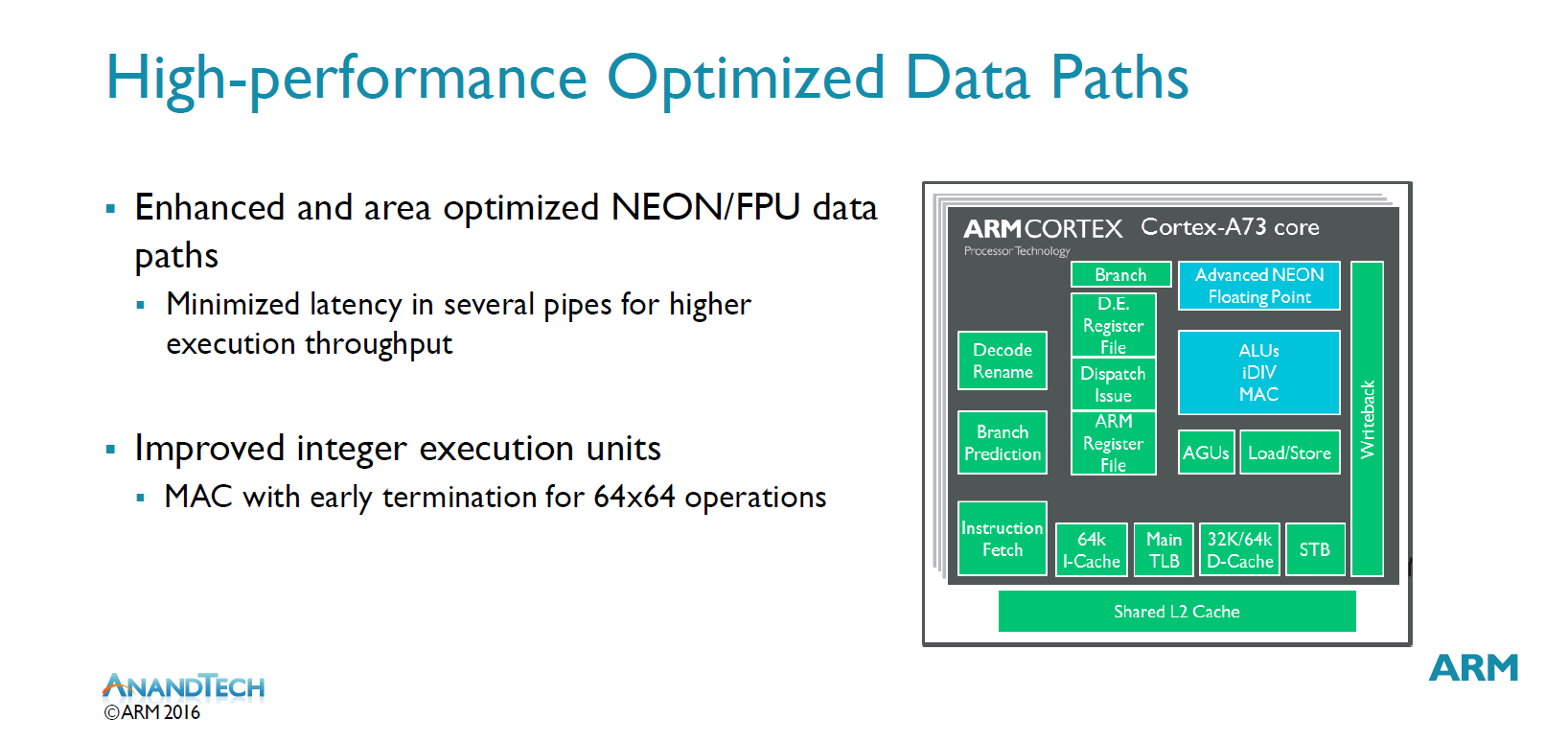
On the data-side when talking about execution pipelines, we don’t see as many improvements as the A73 largely inherits the same NEON units which was introduced on the A72. At last year's TechDay A72 launch we remember ARM stating the new NEON units were brought forward from an advanced future microarchitecture. At the time I had expected this to mean the microarchitecture following the A72, however now ARM unexpectedly tells us that this is a microarchitecture even later than that of the A73. The pulling forward of the NEON units to the A72 is said to have resulted in a lot of learning for the design teams so that we'll actually see even more improvements in the generation following the A73 and even the generation following that. An example of such improvements on the A73 are to be found in miscellaneous FP instructions such as FP transfers and FP moves losing a cycle in some instruction groups. The new NEON units have also seen optimizations to their area usage, making them smaller than in the A72.
The main difference to the A72 lies in the integer units. Instead of 2 basic ALUs with a complex multi-cycle ALU, the A73 sees the latter's capabilities merged into two “beefier” ALUs. Their capabilities isn’t identical: There’s still only one unit which can do division while the other handles multiplication operations. Multiply accumulate operations require both pipelines so this is an degradation compared to the A72 which dedicated such µops to the M pipeline while the two other simple ALUs were free to do other work. The change however also has positive effects as µops for saturating and parallel arithmetic and some miscellaneous data-processing instructions benefit from a doubling in maximum execution throughput.
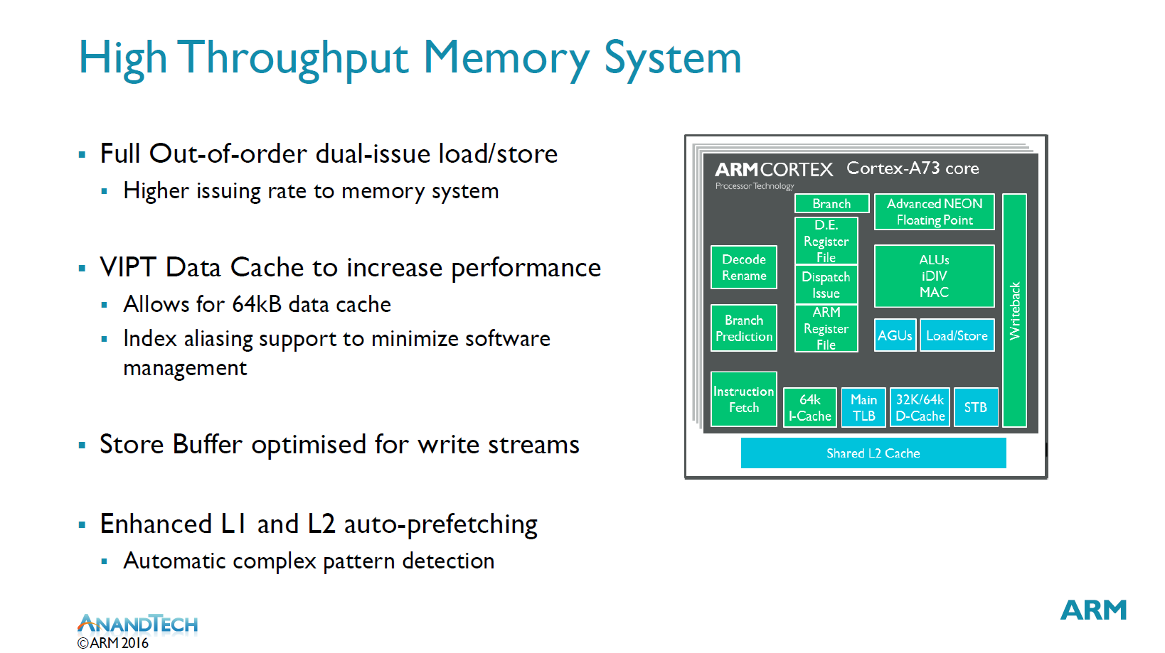
More important than any of the previous aspects of a microarchitecture is the memory system. Again the dual-issue load/store units play a big role in enabling a higher issuing rate into the memory system. The data cache has switched from a PIPT (Physical Index Physical Tag) to a VIPT (Virtual Address Physical Tag) address translation. In a PIPT implementation the largest encountered problem was the translation of addresses to produce indexes, which is one most critical paths of the CPU core. VIPT does away with this problem and also allows for an extended 64KB data cache, up from 32KB on the A17 and A72. ARM claims the larger cache brings an overall 4% performance uplift compared to 32KB. 64KB is the default D-cache size on the A73. Usually software needs to deal with aliasing issues when using VIPT, however the A73 is able to do this in hardware. In hardware the cache is implemented with 4-way associativity but the software sees it as a PIPT 8-way 32kB or 16-way 64KB cache.
A lot of time has been spent on improving the L1 and L2 prefetchers which are large stride based and meant to increase stream performance. Furthermore for irregular patterns there’s the use of an additional prefetcher specialized for the task. ARM is very happy with streaming performance as it’s able to reach near maximum theoretical achievable bandwidth.
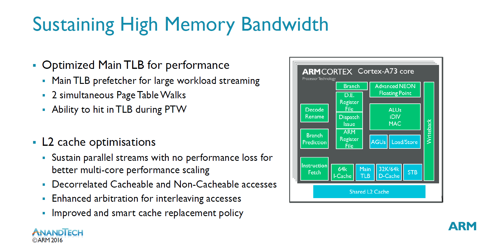
To sustain the improved memory bandwidth there’s also been improvements to the main TLB. In previous microarchitectures large datasets caused performance drops when having to switch to the main TLB. The A73 resolves this issue by giving the main TLB its own prefetchers which allows for sustainable streaming performance even for large data-sets.
On the L2 ARM also improved the resource sharing between CPUs in a cluster. Each CPU has its own dedicated resources so that 1 core streaming will not starve other cores, which enables for parallel streams without performance loss.
Overall in terms of microarchitecture ARM tried to squeeze out the most which is possible out of a 2-wide microarchitecture. We went over what seemed to be some much welcomed improvements to the microarchitecture, but we still need to put it all into context with some performance numbers.


63 Comments
View All Comments
jjj - Monday, May 30, 2016 - link
Chances are Qualcomm will go FOWLP soon and that's why they want custom A73. On 10nm the die will be tiny and plenty of room to add the DRAM in the same package.StrangerGuy - Monday, May 30, 2016 - link
A72s @ 28nm are already scoring ~1700 Geekbench ST. If A73 on the 28nm adds a conservative 20% puts it in Kyro/Mongoose territory. 14nm A73 would be even stronger still with inherent finfet power efficiency boosts.Not hard to see why custom ARM camp should be really worried, because ARM own designs have the flexibility in process nodes while performance is rapidly catching up with custom.
Shyamkr - Monday, May 30, 2016 - link
Is there any comparative data between A73 and qcom kryo cores?phoenix_rizzen - Monday, May 30, 2016 - link
2016 / 2017 are going to be interesting again in the mobile SoC space.We have the fully custom SoCs from the likes of Qualcomm (Kryo CPU, and Adreno GPU).
The semi-custom SoCs from the likes of Samsung (Mongoose big cores + Cortex-A53 LITTLE cores, and Mali GPU) and Apple (Twister CPU, and PowerVR GPU).
The pure ARM SoCs from the likes of MediaTek, Rockchip, Huewai (sp?), and similar (Cortex-A72/A73 + Cortex-A53/A35 and Mali GPUs).
All on multiple processes (28nm, 16nm, 14nm, high-performance, low-power, FinFETT, etc).
Now we just need someone to combine a high-performance, high-efficiency SoC with a high-efficiency radio and screen (that's not too big) and stick a huge battery inside (4000 mAh should be the new normal; anything under 3000 mAh should be avoided). The era of 2-days-between-charges could be upon us ... so long as the OEMs don't squander the battery savings by making the phones even thinner than they are now!!
2015 may have been boring. But it's certainly not anymore!
aryonoco - Monday, May 30, 2016 - link
I also don't think this will be the last of ARM's big core microprocessor family (A15, A57, A72). As the A73 is purely focused on the consumer market, and that's a good thing. However I don't think ARM is giving up on industrial usage and its dream of breaking into the server market. I expect there will be a successor to the A72, and now that it doesn't have to pretend to want to be used in a mobile phone, it can go bigger and wider. It will probably be named something like Cortex A82 or A92 or something, and it could be an absolute beast in Chromebooks, laptops, and potentially maybe even some micro servers. It would be great competition to Intel's Core m, at a fraction of the price.Fun times to be a microprocessor nerd, fun times!
Thanks Andrei for your great reporting. You are making me almost not miss Anand anymore :-)
radar25 - Monday, May 30, 2016 - link
Great Post, I love this articleradar25 - Monday, May 30, 2016 - link
Great Post, dailyplus3 .wix.com/ I love this articleBwash82 - Monday, May 30, 2016 - link
This seems like an awesome replacement for the A72 but why would you need an A53 now. If two A73s can do more with the same space and power budget as 4 A53s why use the core? Honestly I'm kinda mad this was not the core that was initially pushed as the 64 bit chip. ARM was in a great place with the A17 then they pushed forward with a core that was too big hot and power hungry for mobile devices. Honestly I would love to see what a manufacturer can do with six of these bad boys on a soc. May be overkill but it could be fun.saratoga4 - Tuesday, May 31, 2016 - link
A53 perf/watt is much better than the A72. Take a look at the Kirin 950 results. You can more or less double your efficiency with an A53 vs downclocking an A72.fanofanand - Tuesday, September 20, 2016 - link
He was referencing the A73 not the A72. The A73 has nearly the same efficiency as A53 based on the graph, certainly 2 A73's would use less power than 4 A53's, if the graph is to be believed.