Early AMD Zen Server CPU and Motherboard Details: Codename ‘Naples’, 32-cores, Dual Socket Platforms, Q2 2017
by Ian Cutress on August 18, 2016 11:40 PM EST- Posted in
- CPUs
- AMD
- Motherboards
- Enterprise
- Enterprise CPUs
- Zen
- Naples
At the AMD Zen microarchitecture announcement event yesterday, the lid was lifted on some of the details of AMD’s server platform. The 32-core CPU, codename Naples, will feature simultaneous multithreading similar to the desktop platform we wrote about earlier, allowing for 64 threads per processor. Thus, in a dual socket system, up to 128 threads will be available. These development systems are currently in the hands of select AMD partners for qualification and development.
AMD was clear that we will expect to hear more over the coming months (SuperComputing 2016 is in November 2016, International SuperComputing is in June 2017) with a current schedule to start providing servers in Q2 2017.
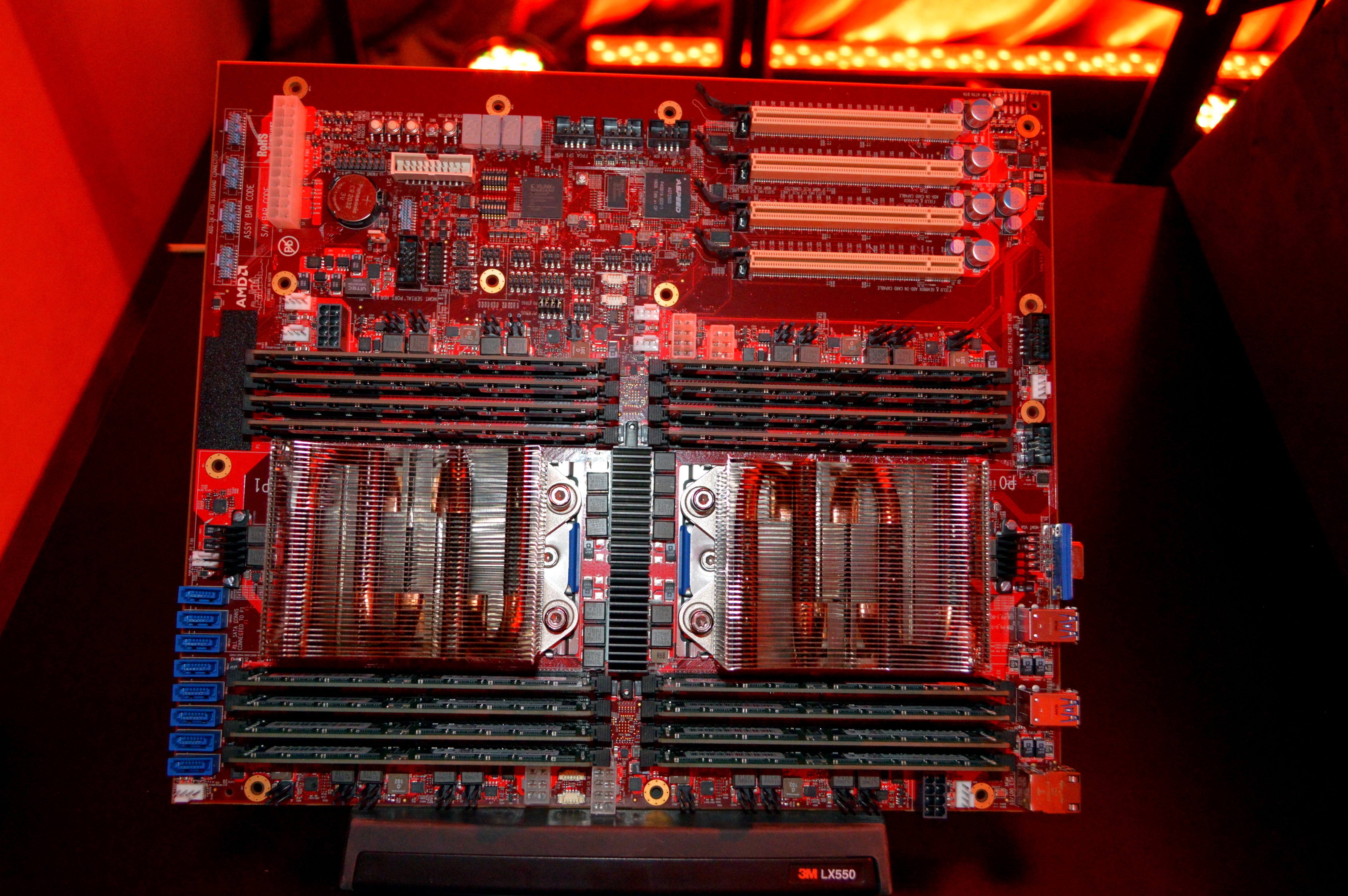
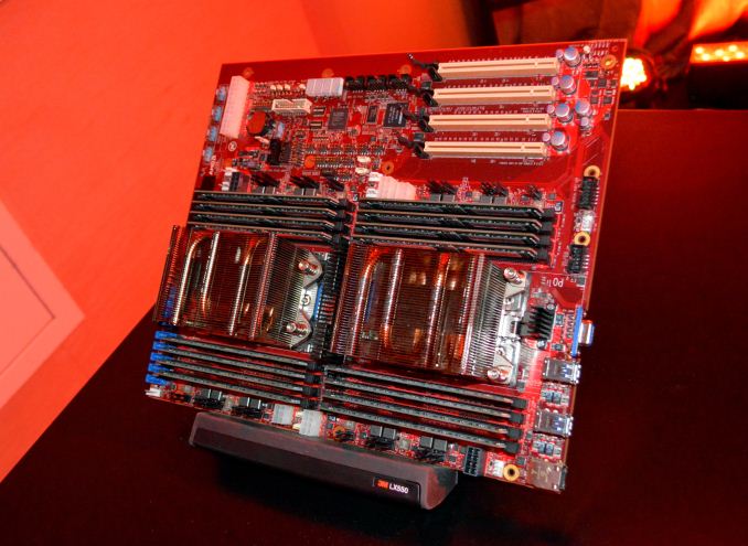
Analysing AMD’s 2P Motherboard
AMD showed off a dual socket development motherboard, with two large AMD sockets using eight phase power for each socket as well as eight DDR4 memory slots.
It was not stated if the CPUs supported quad-channel memory at two DIMMs per channel or eight channel memory at this time, and there’s nothing written on the motherboard to indicate which is the case – typically the second DIMM slot in a 2DPC environment is a different color, which would suggest that this is an eight-channel design, however that is not always the case as some motherboard designs use the same color anyway.
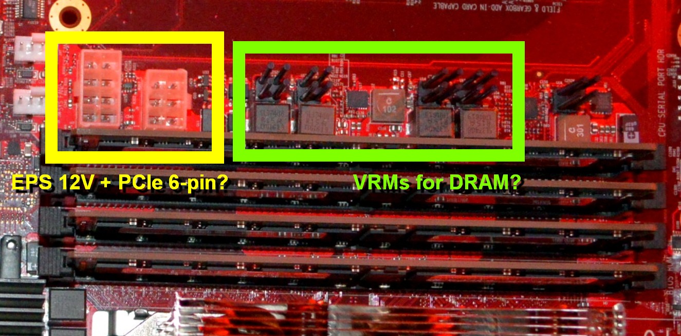
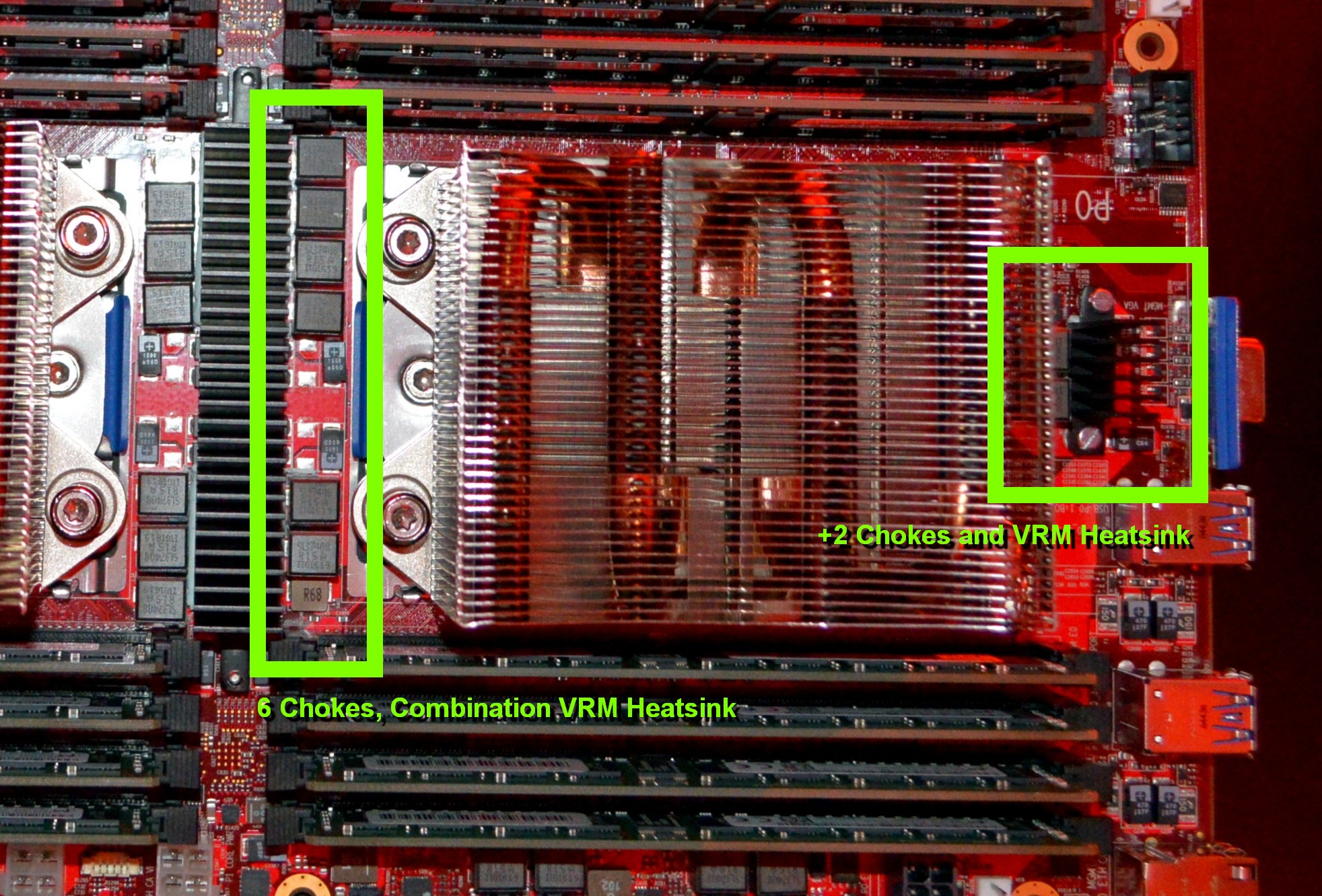
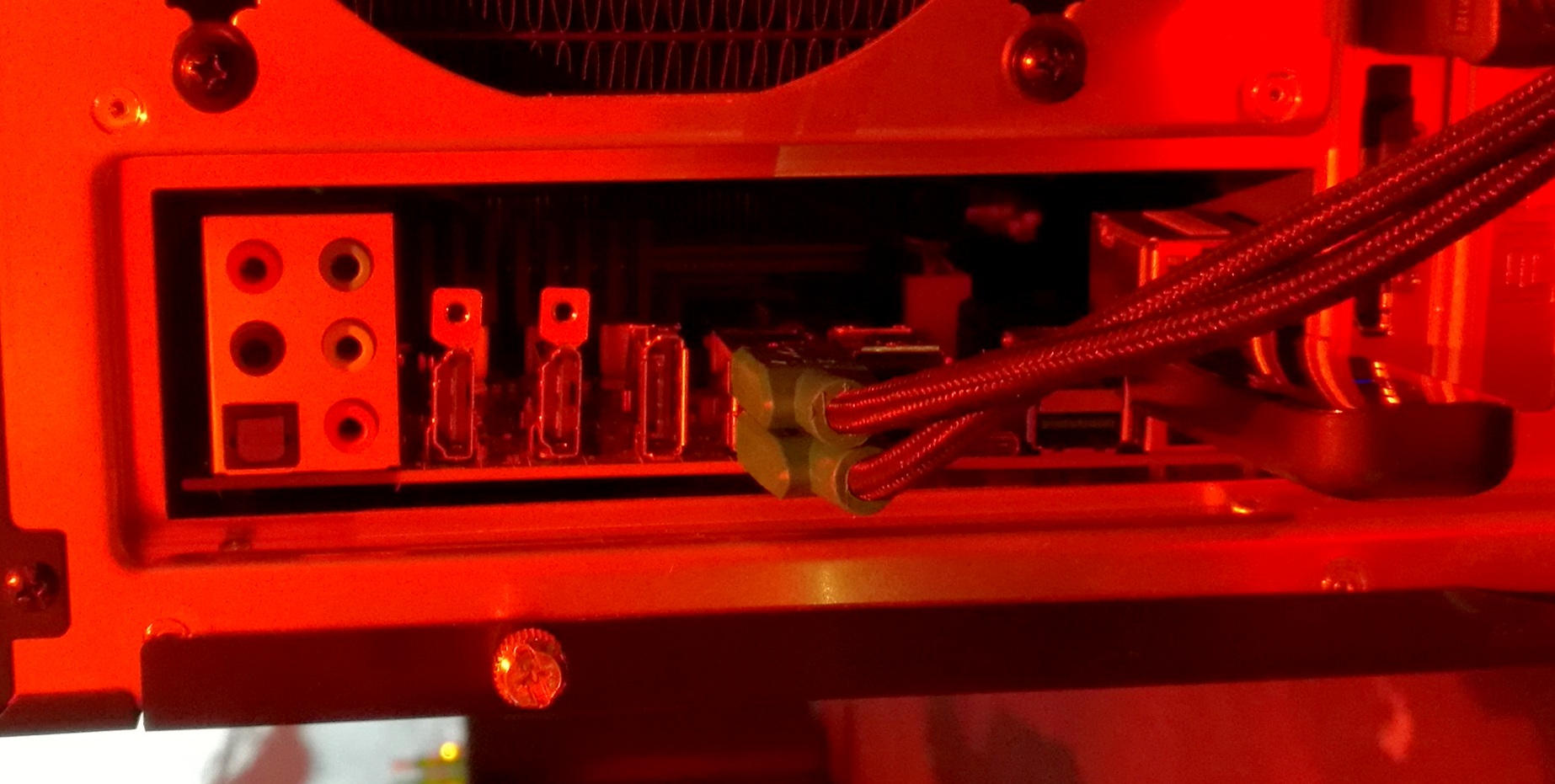
However, it is worth noting that each bank of four memory slots on each side of each CPU has four chokes and four heatsinks (probably VRMs) in two sets. Typically we see one per channel (or one per solution), but the fact that each socket seems to have eight VRMs for the memory would also lean into the eight-channel idea. To top it off, each socket has a black EPS 12V (most likely for the CPU), which is isolated and clearly for CPU power, but also a transparent EPS 12V and a transparent 6-pin PCIe connector. These transparent connectors are not as isolated, so are not for low power implementation, but each socket does have one attached, perhaps suggesting that the memory interfaces are powered independently to the CPU. More memory channels would require more power, and four-channel interfaces have been done and dusted before via the single EPS 12V, so requiring even more power raises questions. I have had word in my ear that this may be as a result of support for future high energy memory, such as NVDIMM, although I have not been able to confirm this.
Edit: The transparent EPS 12V could be a PCIe 8-pin in retrospect, but still seems excessive for the power it can provide.
Unfortunately, we could not remove the heatsinks to see the CPUs or the socket, but chances are this demo system would not have CPUs equipped in the first place. Doing some basic math based on the length of a DDR4 module, our calculations show that the socket area (as delineated by the white line beyond the socket) is 7.46 cm x 11.877 cm, to give an area of 88.59 cm2. By comparison, the heatsink has an active fin floor plan area of 62.6 cm2 based on what we can measure. Unfortuantely this gives us no indication of package area or die area, both of which would be more exciting numbers to have.
Putting the CPU, memory and sockets aside, the motherboard has a number of features worth pointing out. There is no obvious chipset or southbridge in play here. Where we would normally expect a chipset, we have a Xilinx Spartan FPGA without a heatsink, although I would doubt this is the chipset based on the fact that there is an ‘FPGA Button’ right above it and this is most likely to aid in some of the debugging elements on the system.

Further to this, the storage options for the motherboard are all located on the left hand side (as seen) right next to one of the CPUs. Eight SATA style ports are here, all in blue which usually indicates that these are part of the same head controller, but also part of the text on the motherboard states ‘ALL SATA CONNS CONNECTED TO P1’ which indicates the first processor (from the main image, left to right, athough P1 is actually the 'second processor') has direct control.
Other typical IO on the rear panel such as a 10/100 network port (for the management) and the USB 3.0 ports are next to the second processor, which might indicate that this processor has IO control over these parts of the system. However the onboard management control, provided by an ASpeed AST2500 controller with access to Elpida memory, is nearer the PCIe slots and the Xilinx FPGA.
The lack of an obvious chipset, and the location of the SATA ports, would point to Naples having the southbridge integrated on die, and creating an SoC rather than a pure CPU. Bringing this on die, to 14nm FinFET, will allow the functions to be in a lower power process (historically chipsets are created at a larger lithography node to the CPU) as well as adjustments in bandwidth and utility, although at the expense of modularity and die area. If Naples has an integrated chipset, it makes some of the findings on the AM4 platform we saw at the show very interesting. Either that or the FPGA is actually used for the developers to change southbridge operation on the fly (or that chipsets are actually becoming more like FPGAs, which is more realistic as chipsets move to PCIe switch mechanisms).
There are a lot of headers and jumpers on board which won’t be of much interest to anyone except the platform testing, but the PCIe layout needs a look. On this board we have four PCIe slots below one of the CPUs, each using a 16 lane PCIe slot. By careful inspection of the pins we can certainly tell that the slots are each x16 electrical.
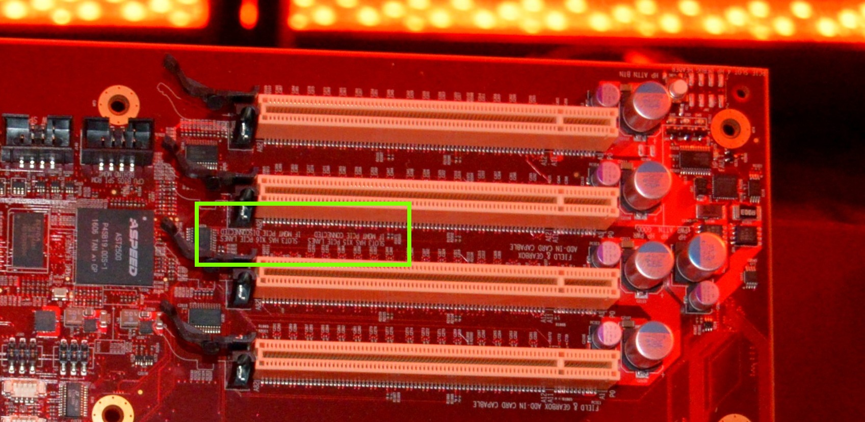
However the highlighted box gives some insight into the PCIe lane allocation. The text says:

“Slot 3 has X15 PCIe lanes if MGMT PCIe Connected
Slot 3 has X16 PCIe lanes if MGMT PCIe Disconnected”
This would indicate that slot three has a full x16 lane connection for data, or in effect we have 64 lanes of PCIe bandwidth in the PCIe slots. That’s about as far as we can determine here – we have seen motherboards in the past that take PCIe lanes from both CPUs, so at best we can say that in this configuration that the Naples CPU has between 32 lanes and 64 lanes for a dual processor system. The board traces, as far as we were able to look at the motherboard, did not make this clear, especially when this is a multi-layer motherboard (qualification samples are typically over-engineered anyway). There is an outside chance that the integrated southbridge/IO is able to supply an x16 combination PCIe lane, however there is no obvious way to determine if this is the case (and is not something we’ve seen historically).
AM4 Desktop Motherboards
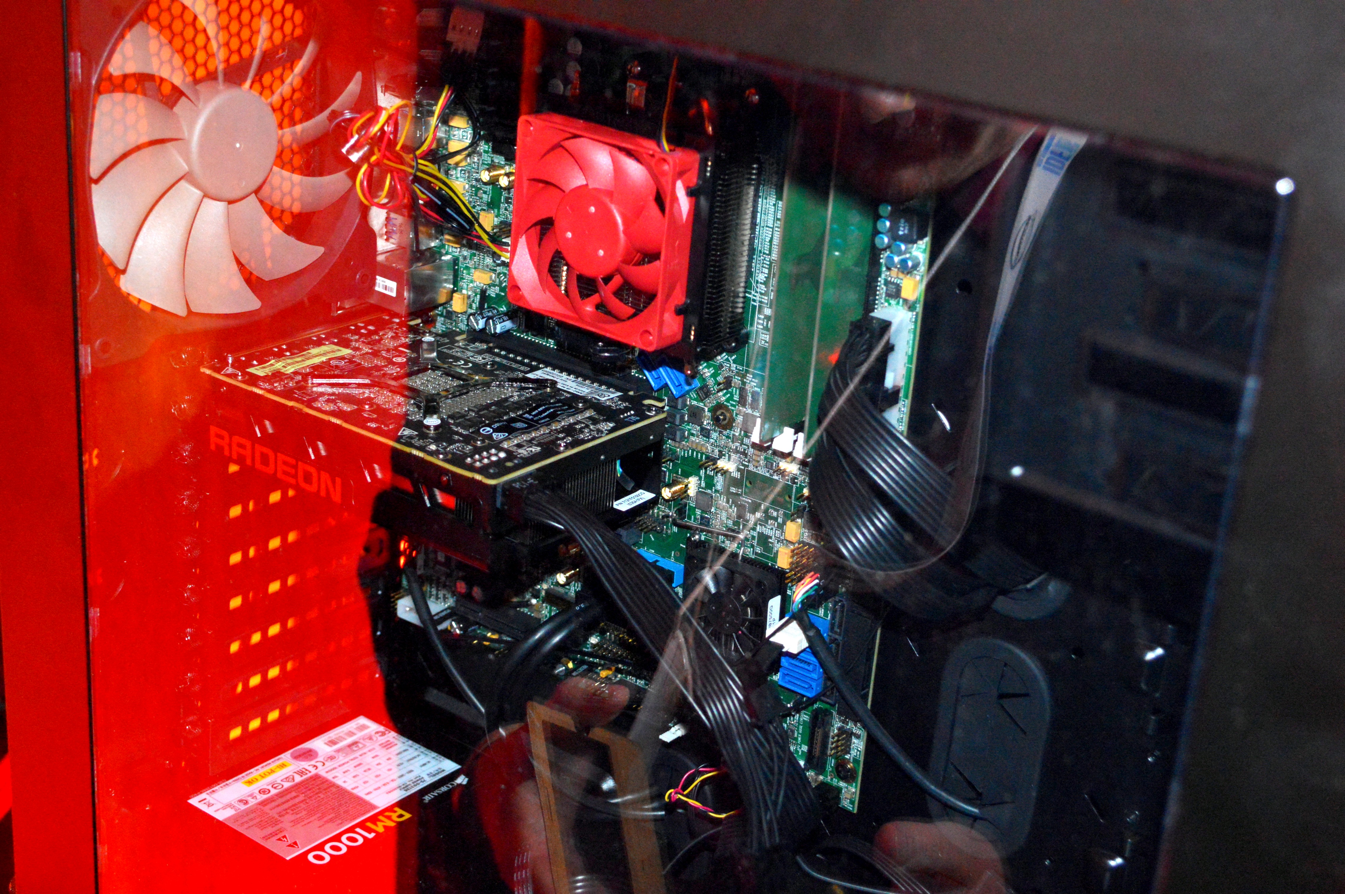
Elsewhere on display for Zen, we also saw some of the internal AM4 motherboards in the base units at the event.
These were not typical motherboard manufacturer boards from the usual names like ASUS or GIGABYTE, and were very clearly internal use products. We weren’t able to open up the cases to see the boards better, but on closer inspection we saw a number of things.
First, there were two different models of motherboards on show, both ATX but varying a little in the functionality. One of the boards had twelve SATA ports, some of which were in very odd locations and colors, but we were unable to determine if any controllers were on board.
Second, each of the boards had video outputs. This would be because we already know that the AM4 platform has to cater for both Bristol Ridge and Summit Ridge, with the former being APU based with integrated graphics and the updated Excavator v2 core design. On one of the motherboards we saw two HDMI outputs and a DisplayPort output, suggesting a full 3-digital display pipeline for Bristol Ridge.
The motherboards were running 2x8GB of Micron memory, running at DDR4-2400. Also, the CPU coolers – AMD was using both its 125W AMD Wraith cooler as well as the new 95W near silent cooler between all four/five systems on display. This pegs these engineering samples at a top end of this TDP, but if recent APU and FX product announcements are anything to go by, AMD is happy to put a 125W cooler on a 95W CPU, or a 95W cooler on a 65W CPU if required.
I will say one thing that has me confused a little. AMD has been very quiet on the chipset support for AM4, and what IO the south bridge will have on the new platform (and if that changes if a Bristol or Summit Ridge CPU is in play at the time). In the server platform, we concluded above that the chipset is likely integrated into the CPU – if that is true on the consumer platform as well, then I would point to the chipset-looking device on these motherboards and start asking questions. Typically the chipset on a motherboard is cooled by a passive heatsink, but these chips here had low z-height on fans them and were running at quite the rate. I wonder if they were like this so when the engineers use the motherboards it means there is more space to plug testing tools, or if it for another purpose entirely. As expected, AMD said to expect more information closer to launch.
Wrap Up
To anyone who says motherboards are boring, well I think AMD has given a number of potential aspects of the platform away in merely showing a pair of these products for server and desktop. Sure, they answer some questions and cause a lot more of my hair to fall out trying to answer the questions that arise, but at this point it means we can start to have a fuller understanding of what is going on beyond the CPU.
As for server based Zen, Naples, depending on PCIe counts and memory support, along with the cache hierarchy we discussed in the previous piece, the prospect of it playing an active spot in enterprise seems very real. Unfortunately, it is still a year away from launch. There are lots of questions about how the server parts will be different, and how the 32-cores on the SKUs that were talked about will be arranged in order to shuffle memory around at a reasonable rate – one of the problems with large core count parts is being able to feed the beast. AMD even used that term in their presentation, meaning that it’s clearly a topic they believe they have addressed.


65 Comments
View All Comments
ZeDestructor - Friday, August 19, 2016 - link
The htansparent one is EPS12V, the black one is PCIe.. looks like more updating needed :PSunLord - Friday, August 19, 2016 - link
I wonder if this points to AMD offering and ability similar to Intel new knights landing socket setup. Maybe A Radeon Pro SSG in P2 using NVDIMMs cause why not go full crazy :Plooncraz - Friday, August 19, 2016 - link
I assume that are to provide all the extra juice they could ever want while overclocking those cores. Engineering boards are usually very heavily overbuilt, this seems to be no exception.And, of course, they will need all that power if they intend to run a few reference RX 480s on it :p
prisonerX - Saturday, August 20, 2016 - link
It's a server motherboard. People run multiple high powered processing units from the PCIe bus and they want ample power via the PCIe ports. Hacks like the PCIe cables you see from ATX PSUs don't cut it in this environment.So the answer is the motherboard doesn't need it, the customers do.
prisonerX - Sunday, August 21, 2016 - link
They're probably for PCIe 4.0 support: http://www.tomshardware.com/news/pcie-4.0-power-sp...ZeDestructor - Monday, August 22, 2016 - link
Yup. Now that that's out and letting the engineers overload (not really) the connectors to push 9A down each pin, pushing the full 1500W though 11 + 2 pins is well within the realm of possibility.I really, really hope this makes it to the consumer end - wire mobo once, never touch power wiring until major mobo upgrades happen...
prisonerX - Monday, August 22, 2016 - link
Now if only motherboards would ditch ATX and start taking a single 12v line...ZeDestructor - Monday, August 22, 2016 - link
Just mention the idea of that and people start raising their pitchforks at Dell/HP/Lenovo for having gone all-12V with Skylake, claiming that it's proprietary, and not good for the consumer, etc.For myself I wish they'd do go all 12V, everywhere, and just move the 3.3V and 5V generation for HDDs to the HDD backplanes (and put backplanes into all cases while they're at it!).
Alexvrb - Tuesday, August 23, 2016 - link
When it's done by OEMs, and they don't all agree on a standard, it IS proprietary! People aren't against going all 12V necessarily. They just want it to be an open standard. Anyway even in the case of the OEMs "all 12V" recent designs, that's just for the PSU - the mainboards supply other voltage outputs to devices as needed. You can't change THAT unless you want to break compatibility with everything you plug into the board.Supposedly it's more efficient this way or something. I think that depends on the PSU, though!
evolucian911 - Monday, August 22, 2016 - link
PCIe 4.0 300-500W power delivery ?