NVIDIA Teases Xavier, a High-Performance ARM SoC for Drive PX & AI
by Ryan Smith on September 28, 2016 7:45 AM EST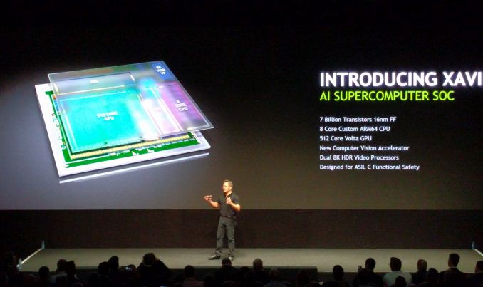
Ever since NVIDIA bowed out of the highly competitive (and high pressure) market for mobile ARM SoCs, there has been quite a bit of speculation over what would happen with NVIDIA’s SoC business. With the company enjoying a good degree of success with projects like the Drive system and Jetson, signs have pointed towards NVIDIA continuing their SoC efforts. But in what direction they would go remained a mystery, as the public roadmap ended with the current-generation Parker SoC. However we finally have an answer to that, and the answer is Xavier.
At NVIDIA’s GTC Europe 2016 conference this morning, the company has teased just a bit of information on the next generation Tegra SoC, which the company is calling Xavier (ed: in keeping with comic book codenames, this is Professor Xavier of the X-Men). Details on the chip are light – the chip won’t even sample until over a year from now – but NVIDIA has laid out just enough information to make it clear that the Tegra group has left mobile behind for good, and now the company is focused on high performance SoCs for cars and other devices further up the power/performance spectrum.
| NVIDIA ARM SoCs | |||
| Xavier | Parker | Erista (Tegra X1) | |
| CPU | 8x NVIDIA Custom ARM | 2x NVIDIA Denver + 4x ARM Cortex-A57 |
4x ARM Cortex-A57 + 4x ARM Cortex-A53 |
| GPU | Volta, 512 CUDA Cores | Pascal, 256 CUDA Cores | Maxwell, 256 CUDA Cores |
| Memory | ? | LPDDR4, 128-bit Bus | LPDDR3, 64-bit Bus |
| Video Processing | 7680x4320 Encode & Decode | 3840x2160p60 Decode 3840x2160p60 Encode |
3840x2160p60 Decode 3840x2160p30 Encode |
| Transistors | 7B | ? | ? |
| Manufacturing Process | TSMC 16nm FinFET+ | TSMC 16nm FinFET+ | TSMC 20nm Planar |
So what’s Xavier? In a nutshell, it’s the next generation of Tegra, done bigger and badder. NVIDIA is essentially aiming to capture much of the complete Drive PX 2 system’s computational power (2x SoC + 2x dGPU) on a single SoC. This SoC will have 7 billion transistors – about as many as a GP104 GPU – and will be built on TSMC’s 16nm FinFET+ process. (To put this in perspective, at GP104-like transistor density, we'd be looking at an SoC nearly 300mm2 big)
Under the hood NVIDIA has revealed just a bit of information of what to expect. The CPU will be composed of 8 custom ARM cores. The name “Denver” wasn’t used in this presentation, so at this point it’s anyone’s guess whether this is Denver 3 or another new design altogether. Meanwhile on the GPU side, we’ll be looking at a Volta-generation design with 512 CUDA Cores. Unfortunately we don’t know anything substantial about Volta at this time; the architecture was bumped further down NVIDIA’s previous roadmaps for Pascal, and as Pascal just launched in the last few months, NVIDIA hasn’t said anything further about it.
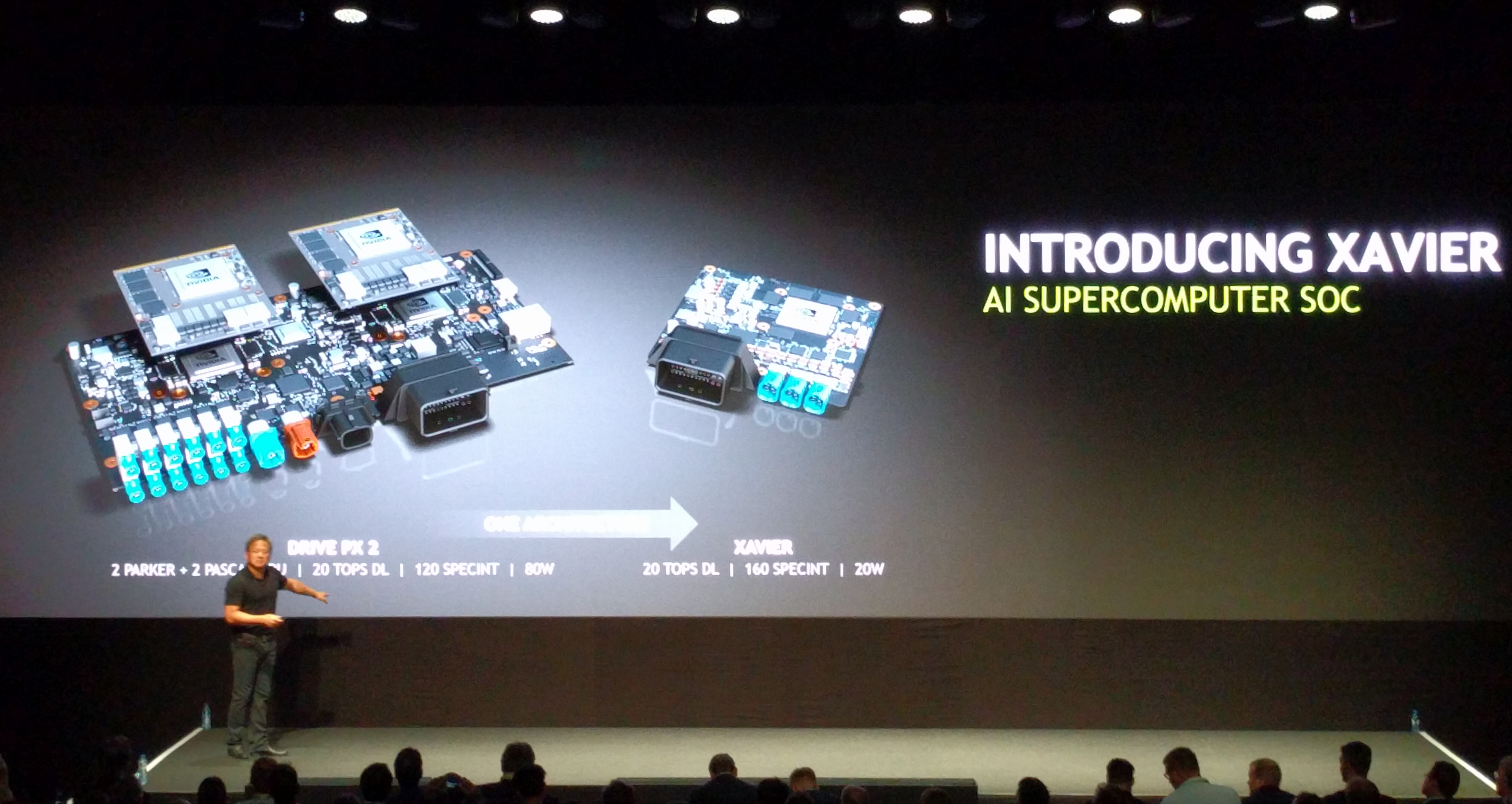
Meanwhile NVIDIA’s performance expectations for Xavier are significant. As mentioned before, the company wants to condense much of Drive PX 2 into a single chip. With Xavier, NVIDIA wants to get to 20 Deep Learning Tera-Ops (DL TOPS), which is a metric for measuring 8-bit Integer operations. 20 DL TOPS happens to be what Drive PX 2 can hit, and about 43% of what NVIDIA’s flagship Tesla P40 can offer in a 250W card. And perhaps more surprising still, NVIDIA wants to do this all at 20W, or 1 DL TOPS-per-watt, which is one-quarter of the power consumption of Drive PX 2, a lofty goal given that this is based on the same 16nm process as Pascal and all of the Drive PX 2’s various processors.
NVIDIA’s envisioned application for Xavier, as you might expect, is focused on further ramping up their automotive business. They are pitching Xavier as an “AI Supercomputer” in relation to its planned high INT8 performance, which in turn is a key component of fast neural network inferencing. What NVIDIA is essentially proposing then is a beast of an inference processor, one that unlike their Tesla discrete GPUs can function on a stand-alone basis. Coupled with this will be some new computer vision hardware to feed Xavier, including a pair of 8K video processors and what NVIDIA is calling a “new computer vision accelerator.”
Wrapping things up, as we mentioned before, Xavier is a far future product for NVIDIA. While the company is teasing it today, the SoC won’t begin sampling until Q4 of 2017, and that in turn implies that volume shipments won’t even be until 2018. But with that said, with their new focus on the automotive market, NVIDIA has shifted from an industry of agile competitors and cut-throat competition, to one where their customers would like as much of a heads up as possible. So these kinds of early announcements are likely going to become par for the course for NVIDIA.


35 Comments
View All Comments
name99 - Wednesday, September 28, 2016 - link
7 billion is not THAT many transistor, just to calibrate expectations.The Apple A10 has 3.3B, at 125sq mm 16nm FF+.
The A10X will probably crack 4B, maybe 4.5B, since it's apparently going to ship on TSMC 10nm early'ish next year, and will presumably at the very least bump up the GPUs by around 50% and, who knows, maybe even add a third core?
The A11X will ship at likely the same sort of time frame (early 2018), quite possibly even on 7nm, and quite possibly approaching the same number of transistors (though on a substantially smaller piece of silicon).
(What will Apple do with all those transistors? Who the heck knows? Maybe just keep upping the GPUs and using them for AI-related matters, the way nV does? Or maybe add specific dedicate AI hardware of the sort pioneered by Movidius and Nervana?)
Krysto - Wednesday, September 28, 2016 - link
I mean, the chip looks very impressive for what it is, but it's getting a little annoying seeing Nvidia name everything from a $200 chip to a $129,000 one an "AI supercomputer".This performance of this chip will likely still be a tiny fraction of what Level 4 autonomous driving systems will require 10 years from now, so why call it a supercomputer, as if it's already more than capable of handling Level 4 self-driving or whatever?
What are they going to call their 2020 generation? The "AI Quantum Computer" (but you know, without actually being a quantum computer either...)
Meteor2 - Wednesday, September 28, 2016 - link
Did you read the live blog? This looks enough for Level 4, easily.GhostOfAnand - Wednesday, September 28, 2016 - link
Yawn...djayjp - Wednesday, September 28, 2016 - link
8K video but not at 60fps?Yojimbo - Wednesday, September 28, 2016 - link
That chart was made by Anandtech based on all information they know. The Parker and Erista entries are filled from published information on existing products. The Xavier entries are filled from slides from a keynote presentation giving a 'sneak-peak' of the architecture. Trying to compare the different entries too critically is bound to result in red herrings.Yojimbo - Wednesday, September 28, 2016 - link
Well I'm gonna take a wild guess even though I have a very limited knowledge of the industry. The two surprising numbers are 7 billion transistors and 20 DL TOPS at 20 W. A 512 core Pascal GPU would be about 2 billion transistors by my very rough estimate. I think that leaves three possibilities: 1) Volta has a massive increase in transistor per core over Pascal in general 2) the GPU in Xavier must be specially designed or 3) over 2/3 of the transistors are devoted to other areas of the chip.I can't see number 1 happening because the GV100 looks to have 1.6 to 2 times the theoretical performance of the GP100 on the same process node. The GP100 is already a physically maxed out chip, so they would not be likely to be able to have such a huge transistor count increase without reducing the number of CUDA cores on the GV100 is compared with the GP100. Then, the GV100 would need to either run at vastly higher clocks or perform more than 2 FMA per clock in order to achieve its performance. Both seem unlikely.
That leaves 2) or 3). I think they are just different ways of saying the same thing. There is specialized hardware on the SOC for performing DL operations, outside the realm of a normal GPU, and there are a significant number of transistors on Xavier devoted to it. There are 4 blocks mentioned on NVIDIA's slides. The GPU block, the CPU block, "dual 8k HDR video processors", and a "computer vision accelerator". My guess is that an "HDR video processor" is more than just encode/decode block and includes an ISP. If so then what the computer vision accelerator does is a mystery to me (though maybe not to someone with knowledge about vision processing). I propose that this computer vision accelerator is a special compute unit that consists of a significant number of transistors (>2 billion?) and accounts for a significant number of DL TOPS (>10 DL TOPS?).
Yojimbo - Wednesday, September 28, 2016 - link
I meant "more than 2 FP ops per core per clock", not "more than 2 FMA per clock".syxbit - Wednesday, September 28, 2016 - link
It's really sad that they're not doing mobile SoCs. I get they've had some terrible chips (T2, T3 and the 64-bit K1), but the T4 was okay. The 32-bit K1 was very good, and the X1 was the best Android SoC of 2015. I'd love to see this Xavier in a Shield TV2 (or other Shield device).I'd really like it if they designed their new stuff with the ability to downsize. Have an 8 core beast for AI, but chop it down to size and give us a 2-4 core Tablet chip.
A5 - Wednesday, September 28, 2016 - link
They couldn't get any phone design wins from major OEMs. Android tablets aren't a big enough space to justify the resources they were putting in.