Samsung Foundry Announces 10nm SoC In Mass-Production
by Andrei Frumusanu on October 17, 2016 5:40 AM EST- Posted in
- Semiconductors
- Samsung
- fabrication
- 10LPE
Today Samsung announced mass production of a SoC built on its third-generation 10nm "10LPE" manufacturing node. It was only this January that Samsung announced mass production of its 14LPP process that ended up being used in the Exynos 8890 and the Snapdragon 820 powering up a large amount of flagship devices this year.
This time around the announcement comes quite early compared to the past 2 years and I wasn't expecting any news from the foundry till maybe later in the quarter. This does however bode well for the SoCs built on the process as they seem they'll be able to easily make the spring 2017 device release schedule.
There wasn't any specification as to what kind of SoC the mass production announcement is refering to, but it's very likely we're talking about S.LSI's next generation Exynos - or maybe even Qualcomm's Snapdragon 820 successor, both of which we'll hopefully hear official announcements from in the coming months.
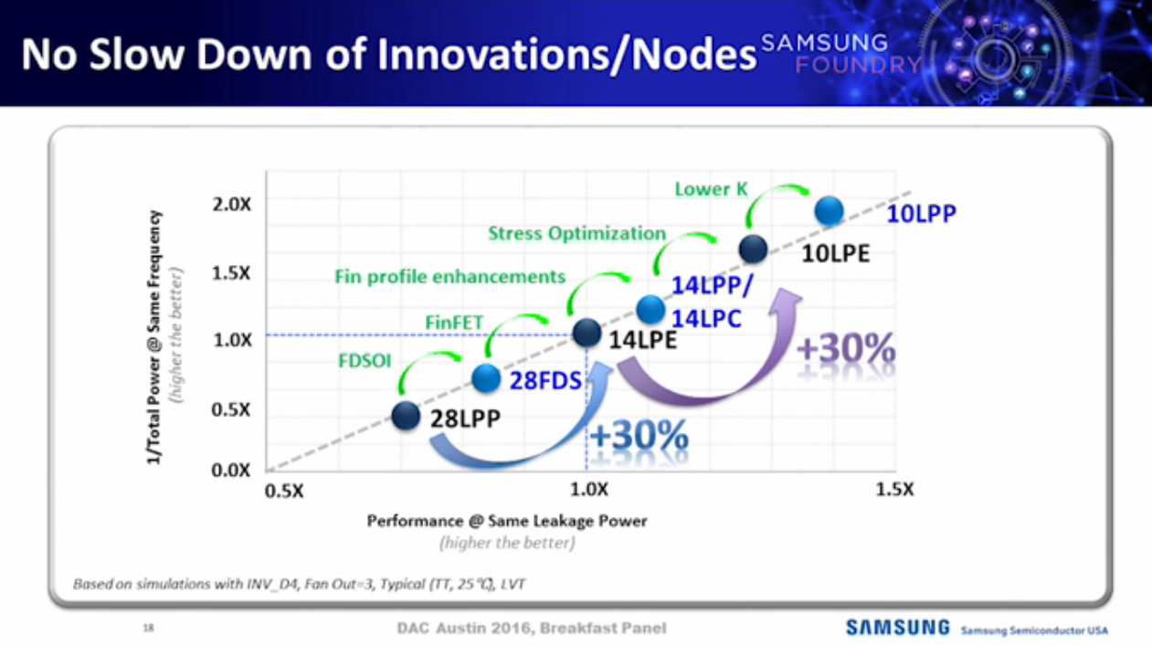
Samsung’s new 10nm FinFET process (10LPE) adopts an advanced 3D transistor structure with additional enhancements in both process technology and design enablement compared to its 14nm predecessor, allowing up to 30-percent increase in area efficiency with 27-percent higher performance or 40-percent lower power consumption. In order to overcome scaling limitations, cutting edge techniques such as triple-patterning to allow bi-directional routing are also used to retain design and routing flexibility from prior nodes.
Credit: DAC 2016 Samsung/Synopsys Breakfast - Ready to Design at 10nm!
The process promises some significant speed and power efficiency advantages over current generation designs so it's likely the next generation of devices will see a large boost, similarly to how the first 14/16 SoCs had large improvements over previous generation 20/28nm designs.
Interestingly the new SoCs will have an edge on recent and upcoming designs still being released on 16nm manufacturing processes, such as Apple's A10 or other TSMC customers who have to wait till next year for 10FF. This presents itself as an opportunity for vendors such as Samsung and Qualcomm to try to close the performance and efficiency gap seen in the current generation through the manufacturing process' good timing.
Source: Press Release


92 Comments
View All Comments
close - Monday, October 17, 2016 - link
If there was "nothing in a 10nm node that measures 10nm" we'd already have 5 or 2nm nodes. Maybe even smaller. Don't underestimate the ability with which marketing departments fail to understand technical details. This is why in this particular case all marketing terms are actually tied to an engineering concept: feature size. The node is the smallest feature that you actually have on the die. ...With the obvious and hopefully reasonable approximations.witeken - Tuesday, October 18, 2016 - link
I'm sorry to disappoint you, but you are a little bit naieve. Node names ARE marketing. They used to be engineering names, but marketing hijacked them. So the rule is to shrink the name by 0.7x every generation. So that's what marketing still does. However, they do this even if the feature size does not in fact shrink by 0,7x. 14nm is the same density as foundries' 20nm.So again, please go to Wikichip and find me a feature size that is 14nm. You can't because there is none.
name99 - Monday, October 17, 2016 - link
Even more to the point, if any foundry has higher density, so what? Higher density does not automatically correlate with higher performance, lower cost, or anything else that an end user actually cares about.Higher density mattered years ago, when it was a struggle to fit everything we wanted on a single die. But now we have so many transistors we just burn them up with yet another core, or throw in another few MB of cache. What's of interest is either the details that affect price (how many steps required to achieve various functionalities), the details that affect design (whether 2D routing can be used, where double or triple patterning is necessary), and the details that affect performance (precise properties of the transistors, how many metal layers, whether advanced materials or air gaps are available).
The reason (IMHO) the foundries are so happy to let people know about density is precisely because it is so meaningless --- revealing it is not revealing any secret that actually matters worth a damn.
witeken - Tuesday, October 18, 2016 - link
Completely incorrect. Intel has in fact the highest yields in the industry -- Intel's 22nm is in fact their best yielding node EVER. Stop the FUD, please get your facts straight by using reliable sources.bcronce - Monday, October 17, 2016 - link
13.3nm is 10% denser than 14nm. Kind of lends credence to Samsung 10nm = Intel 14nm.lefty2 - Monday, October 17, 2016 - link
It's close, but it's not equal. 10% is 10%Meteor2 - Monday, October 17, 2016 - link
One exists (Intel) the other is 'announced' (Samsung). That leaves Intel with a rather large advantage.bcronce - Monday, October 17, 2016 - link
Except when you include arbitrary forms of roundingCygni - Monday, October 17, 2016 - link
Those values, especially for future processes that they have no hard data on (like, say, Samsungs 10nm), are pure estimations. At best.lefty2 - Monday, October 17, 2016 - link
I'm told that they created that table using technical data released by the foundries that specifies the metal pitch etc.