Samsung Foundry Announces 10nm SoC In Mass-Production
by Andrei Frumusanu on October 17, 2016 5:40 AM EST- Posted in
- Semiconductors
- Samsung
- fabrication
- 10LPE
Today Samsung announced mass production of a SoC built on its third-generation 10nm "10LPE" manufacturing node. It was only this January that Samsung announced mass production of its 14LPP process that ended up being used in the Exynos 8890 and the Snapdragon 820 powering up a large amount of flagship devices this year.
This time around the announcement comes quite early compared to the past 2 years and I wasn't expecting any news from the foundry till maybe later in the quarter. This does however bode well for the SoCs built on the process as they seem they'll be able to easily make the spring 2017 device release schedule.
There wasn't any specification as to what kind of SoC the mass production announcement is refering to, but it's very likely we're talking about S.LSI's next generation Exynos - or maybe even Qualcomm's Snapdragon 820 successor, both of which we'll hopefully hear official announcements from in the coming months.
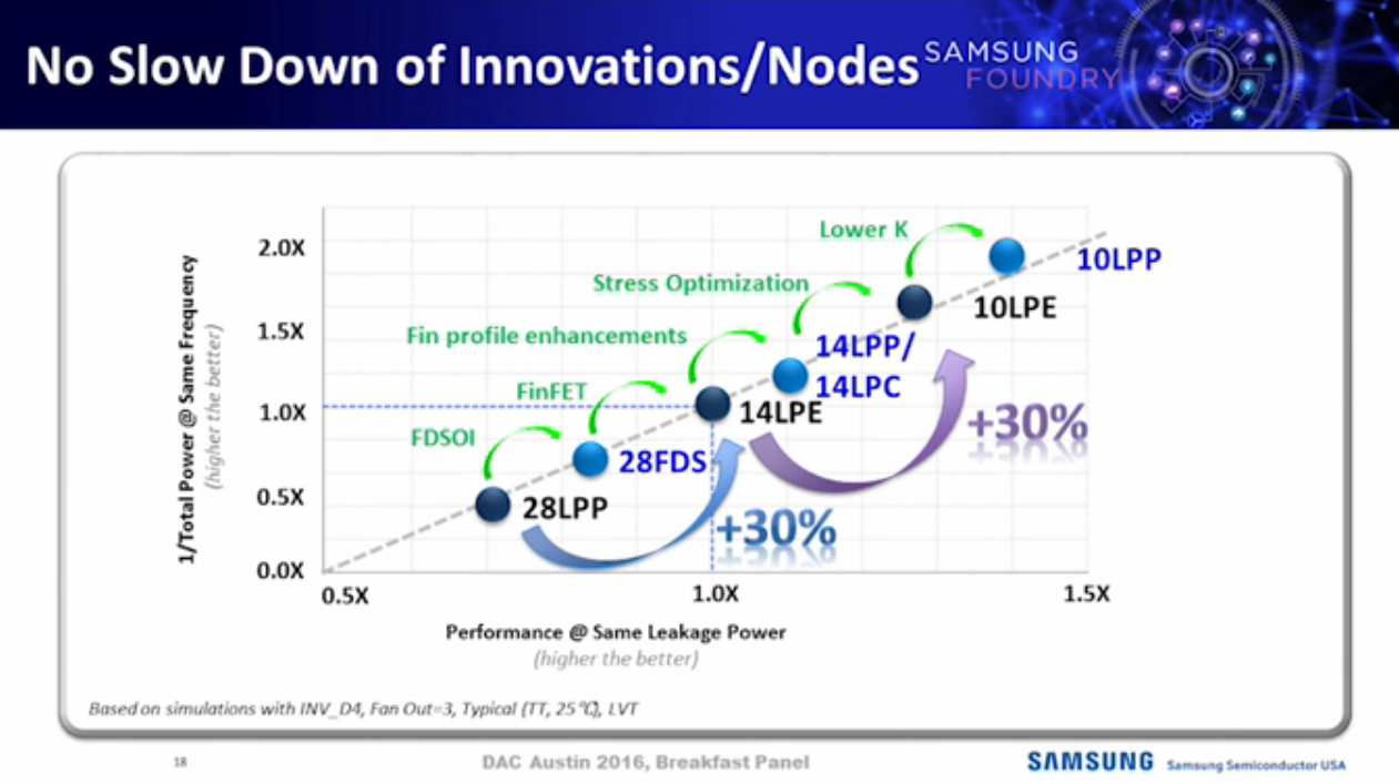
Samsung’s new 10nm FinFET process (10LPE) adopts an advanced 3D transistor structure with additional enhancements in both process technology and design enablement compared to its 14nm predecessor, allowing up to 30-percent increase in area efficiency with 27-percent higher performance or 40-percent lower power consumption. In order to overcome scaling limitations, cutting edge techniques such as triple-patterning to allow bi-directional routing are also used to retain design and routing flexibility from prior nodes.
Credit: DAC 2016 Samsung/Synopsys Breakfast - Ready to Design at 10nm!
The process promises some significant speed and power efficiency advantages over current generation designs so it's likely the next generation of devices will see a large boost, similarly to how the first 14/16 SoCs had large improvements over previous generation 20/28nm designs.
Interestingly the new SoCs will have an edge on recent and upcoming designs still being released on 16nm manufacturing processes, such as Apple's A10 or other TSMC customers who have to wait till next year for 10FF. This presents itself as an opportunity for vendors such as Samsung and Qualcomm to try to close the performance and efficiency gap seen in the current generation through the manufacturing process' good timing.
Source: Press Release


92 Comments
View All Comments
witeken - Tuesday, October 18, 2016 - link
I'm sorry to disappoint you, but they didn't. Well, their are two things here.First, for the nodes up to 14nm, they indeed used correct transistor feature sizes. However, for all lower nodes they used estimates that clearly favor TSMC by a huge margin. For instance, they assume TSMC 10nm will have 2.1 density, while Intel 10nm has 1.6x density. Their is no reliable source for both of these numbers, so they are clearly invented. Let alone 7nm or 5nm.
However, all of this doesn't even matter because the formula they use is just WRONG. If your math is wrong, your output is just worthless.
name99 - Monday, October 17, 2016 - link
The process details are generally pretty well known by now. TSMC, for example, has fabricated working ARM test chips on 10nm. Risk product generally starts about 9 months before products ship; I don't know how things break down, but I imagine it's something like 3 or 4 months of debugging and tweaking what was learned in risk production, then 5 or 6 months of building inventory before the tentpole product (high-end phone or tablet or whatever) launched.Point is, at this stage in the game, Samsung (and TSMC) surely know their process details. They've probably released them at conferences. They certainly released them to partners a year or more ago. So they're hardly secret. They don't need to be "guessed".
medi03 - Monday, October 17, 2016 - link
What marketing? Since when is Intel into fab business? (producing 3rd party chips)name99 - Monday, October 17, 2016 - link
The word you want is not fab business but foundry business.Intel has tried to be in the foundry business for some years now, with notable lack of success and no design wins worth cheering over.
http://www.intel.com/content/www/us/en/foundry/ove...
https://en.wikipedia.org/wiki/Intel#Opening_up_the...
Opinions differ as to why they have been unsuccessful and whether that will change. Like all the best arguments, there are very few actual facts available, so everyone involved can believe what they like...
They're supposed to be manufacturing a custom ARM SoC for LG using their 10nm process. Everything I've read about this is all over the place, the suggestion seems to be (without anyone willing to actually commit to a date) that this part is supposed to "start" next year, with no details as to whether "start" means start the design, start risk production, ship in volume, or ...
witeken - Tuesday, October 18, 2016 - link
NOOOO, I'm sorry for this harsh reaction but do not rely on SemiWiki for information.I have analysed their article 1 month ago and when I did the math -- which they cowardly hide behind their formula -- it turns out to be a complete TSMC PR article. For instance, according to them, Intel's 10nm and 7nm will be only 1.6x denser then their predecessor, which is a completely lie (1) because Intel has not formally announced density of 10nm and hasn't even spoken about 7nm and (2) because what they DID say is that they will make up for the longer time between nodes by shrinking more aggressively, so at least 2X.
name99 - Tuesday, October 18, 2016 - link
Like most people here, you're obsessed with density. I think this is misleading for the purposes most of us care about. Let me try to give my best explanation here (corrections welcome).Consider the following two pictures:
https://en.wikipedia.org/wiki/Multigate_device#FIN...
Look at the picture called "A double-gate FinFET device". This is easy enough to understand. Current flow from source to drain (or the other way round, depending on whether you prefer electrons or positive charge...), in a manner that is controlled by the gate.
Clearly some dimensions of interest here might be the height of the green fin, the width of the green fin, and the distance between the source and drain. In particular, the distance between source and drain should, presumably, have some correlation to transistor switching time, so shrinking it makes the transistor faster.
OK, now look at
http://www.electronics-eetimes.com/news/samsung’s-14-nm-lpe-finfet-transistors/page/0/3
It takes some time to parse this picture, but the parts to compare with the earlier picture are first look for S and D (corresponding to Source and Drain in the previous picture) then the grey interleaving is the gate. The stuff you see that looks like fins is not actually, the fins are thinner and hidden underneath, you see them indicated by the "Si fin direction" arrows.
The smallest dimensions that appear visible are the widths of the grey (gate) and white (source + drain) elements. This dimension is, as far as I can tell, then, what is called the gate length, and tends to be around 1.7 to 2x the "node". This is, again as far as I can tell, the most important dimension for transistor performance (insofar as it facilitates higher frequency switching).
The pitches, then, are the minimum distances between objects [including the width of one of the two objects] (as opposed to the minimum widths of objects). The metal pitch is given as about twice the width, and that seems to track with photo.
This pitch (ie minimum distance between objects) tracks density more closely, in that it limits how many of various things you can place per square micron, but for transistor performance purposes it's probably less interesting than the gate length.
We can't see the fins in this photo, but the fins are SUPPOSED to be 2/3 (or thiner) the so called gate length. (Which, remember, is, in this picture, actually the WIDTH of the grey protrusions).
So I think one could reasonably argue that the fin width (more or less) tracks the node name.
However the actual fin width in these processes seems to be a secret. Even the academic papers I could find didn't mention it.
Note that the gate length, important though it is, is not the only determinant of the transistor speed. The material properties matter for all the constituents of the transistor (its source, drain, gate, the metal contacts, and the precise geometry). Also the transistor speed is not the only determinant of SoC speed; the speed at which signals can travel over the wires between transistors, especially transistors some distance from each other, also matters and is generally, if you're prepared to burn the power to run your chip at high frequency, the limiting factor unless you work to deal with it.
And back to density. That's determined, like I said, not exactly by the size of the smallest objects (presumably the fins) but by the minimum distance between objects, which is a different dimension. It's feasible, for example, to be willing to pay for thin fins and short gate lengths, but not be willing to pay to put them very close together (or what amounts to somewhat of the same thing, not be willing to pay for very narrow metal lines that could connect between transistors that are very close together).
This all makes more sense when you think of it in terms of manufacturing. Each halving of a critical dimension requires a few more finicky manufacturing steps, so if you can get away with not doing that, you're going to.
witeken - Wednesday, October 19, 2016 - link
I am nof necessarily obsessed with density. I also find the other characteristics of a transistor, which you mention, important. However, I don't like it when people don't know the exact sizes and start guessing around without knowledge or led them lead by node names or other crap.Most of your analysis is correct, but I do want to make a few small corrections.
I would have said the gate length is not the ultimate factor that determines speed or power, but you corrected yourself already :). But it is indeed quite an important feature still. So FYI, Intel's 14nm gate length is 20nm, while both Samsung and TSMC have a gate length a bit higher than 30nm.
Another factor that is important for speed if the fin height. For Intel, this was 34nm at 22nm and increased to 42nm at 14nm. The foundries are in between those values with 14/16nm: about 37-38nm.
A last factor that is important for speed and power is the subthreshold slope, which for Intel is 65mV/dec, which is close to the theorectical value of 60mV/dec. If I remember correctly, the slope of a planar transistor is about 100mV/dec.
Next, the features that you try to describe have a specific name, namely fin pitch, gate pitch and interconnect pitch. The best estimate one can make for the transistor area is gate pitch multiplied by gate length: http://www.extremetech.com/wp-content/uploads/2014...
Lastly, the fin width is indeed one of the shortest features, but it is pretty much a constant for finFETs, so it does not follow the node names or anything.
For everyone the fin width is 8nm. This will not changes much if any in the coming nodes.
name99 - Wednesday, October 19, 2016 - link
Pitches are the distance between objects. That's part of my point --- I was interested in the size of objects (information that I found hard to find) not the distances between them.Do you have a reference for that fin width of 8nm? I could not find anything definite except three claims in different places:
- that old-style (two-sided) finFET's required a width of half the gate length
- that tri-gate finFETs (which everyone now uses) required a width of equal to the gate length and
- that finFETs (no distinction as to trigate or not) required a width of 2/3 the gate length.
As for fin height, TSMC have demoed chips that use variable fin height (more precisely the process offers two fin heights, and you can use the taller fins where you need larger currents). The advantage was that density improved quite a bit for some structures because locations that had needed two fins could be replaced with a single taller fin. (Of course this is always modulo issues like assuming the wiring can then be made as dense as needed...)
As always, who knows when that will make it into production. But it certainly suggests that they are on Intel's track and (as always, I guess) looking not just for the performance advantage, but for a level of flexibility beyond what Intel tends to offer.
witeken - Wednesday, October 19, 2016 - link
http://www.intel.com/content/dam/www/public/us/en/...It's right there in the Abstract.
name99 - Wednesday, October 19, 2016 - link
Thanks for the reference. Looks very interesting.