Intel to Equip Fab 42 for 7 nm
by Anton Shilov on February 9, 2017 4:45 PM EST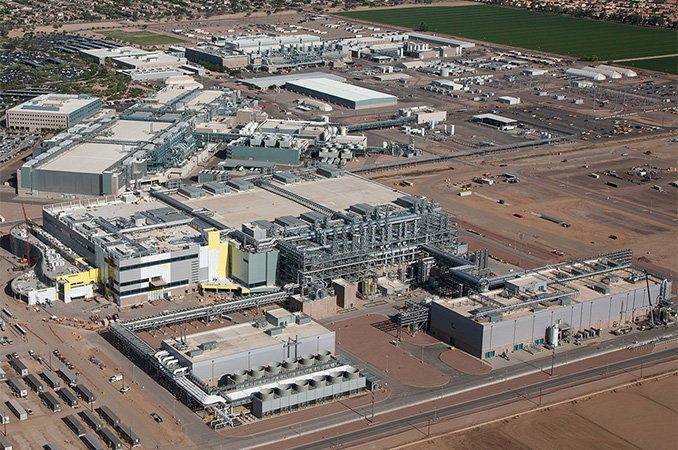
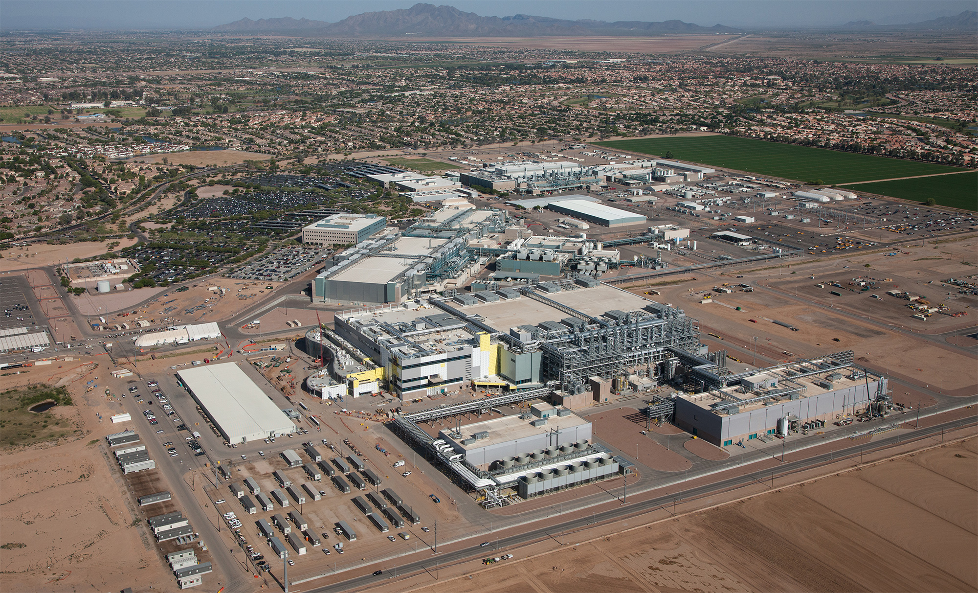
Intel this week announced plans to bring its Fab 42 online to produce semiconductors using a 7 nm fabrication process. It will take three to four years, and the move will cost Intel several billions of dollars but will create approximately 3,000 of high-tech jobs in Chandler, Arizona. Unfortunately, Intel did not share details about its 7 nm manufacturing technology at this time.
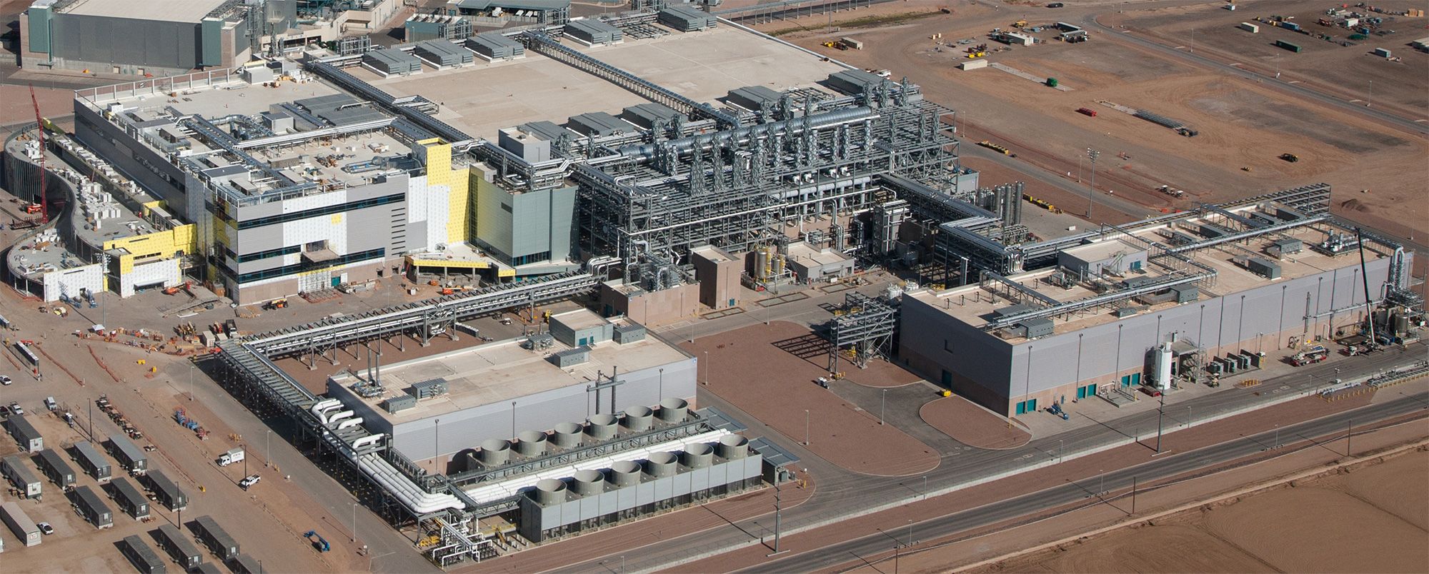
Intel began construction of its Fab 42 back in 2011 with the aim to build the most advanced, high-volume chip production facility in the world. The building was completed in 2013, but instead of moving in equipment to produce chips using 14 nm fabrication process, Intel decided to postpone its completion in early 2014. The site is equipped with heating, air conditioning, and other essential things, but no actual semiconductor manufacturing equipment has been installed. Intel still has no immediate public plans to use the Fab 42 for the production of chips using its 10 nm process technology in the short-term future but has indicated it intends to use it for its 7 nm ICs several years down the road.
Intel intends to spend as much as $7 billion to equip Fab 42, but at the moment the company does not share what kind of tools it plans to install. As a result we have no new information about Intel's 7 nm technology. Intel has implied that it could start using extreme ultraviolet (EUV) lithography at 7 nm, but has never committed to the plan. Earlier this year the company said it would invest in a 7 nm pilot line in one of its development sites, but did not elaborate beyond that. One of the things that the CEO of Intel disclosed about the 7 nm in general in his email to employees this week is that it requires “an increasing amount of factory space per wafer.” This possibly means that Intel will insert EUV equipment into the process technology for cirical layers and will continue to use a lot of multipatterning, which increases the diversity requirements for the production tools.
Intel believes that when completed, Fab 42 will be the most advanced semiconductor wafer fab in the world that will create 3,000 direct high-tech jobs and 10,000 direct and indirect jobs in total. It should be noted that the semiconductor company will not start to move in equipment into the Fab 42 before it figures out all the peculiarities of the 7 nm manufacturing technology. Once it finalizes the pilot line and is satisfied with the equipment performance, it starts to replicate the line at different sites.
Intel said that it will use its 7 nm fabrication process to produce various processors for PCs, data centers and other devices that will be used for AI, automated driving, medical research/treatment as well as other applications. So, as usually, the manufacturing technology will be positioned to make the whole stack of Intel’s products several years from now.
Related Reading:
Source: Intel


24 Comments
View All Comments
kiers - Thursday, February 9, 2017 - link
Does Arizona have the GROUNDWATER to support this kind of Fab in the desert?seerak - Friday, February 10, 2017 - link
How much groundwater does a fab need?I don't actually know the answer to that - but that facility is surrounded by several subdivisions with fake lakes, so there's water to be had.
GibsonSG - Wednesday, March 8, 2017 - link
Should have plenty...mainly due to the National Reclamation Act of 1902 which, over time, has seen a chain of lakes created NorthEast of the metro-Phoenix area to supply the city/state with water. Also, to build or expand, the city or private water company has to prove to the state that they have a 100-year assured water supply. The state/city also make extensive use of recharge and reclaim systems. On top of all that, I believe Chandler's Ocotillo campus has on-site recycling for about 80% or more of the water they use.Intel would never have started FAB 42 to begin with if they didn't have supply assurances, considering the investment cost.
paperfist - Friday, February 10, 2017 - link
What are those lush green fields to the right of the facility?IntelToaster - Friday, February 10, 2017 - link
From what I can see on Google Earth, it looks like agricultural flood irrigation plots. I must be mistaken, as I can't see why anyone would want to use flood irrigation in Arizona, but I couldn't find any further information on it.Refuge - Wednesday, February 15, 2017 - link
Actually fun fact, Arizona is plagued by flash flooding.The ground is too dry and compact to absorb any moisture, so even a short thunderstorm turns into a flash flood within minutes.
Gotta keep dem chips dry!
SkyBill40 - Monday, March 13, 2017 - link
Farm land. There's a lot of corn fields in the area.hrrmph - Friday, February 10, 2017 - link
Enough butchered English. Get this author an editor.zodiacfml - Saturday, February 11, 2017 - link
This is going to take a long, while. On the conversation on performance, it is more about competition which caused the stagnation. We should be using larger die size chips than we have these days.karakarga - Sunday, February 12, 2017 - link
22nm to 10nm fabric cost: 5 billion dollars,7nm and lower fabric cost: 7 billion dollars.
Maybe 3nm and lover fabric cost: 10 billion dollars
Do we also pay "double", after 5~10 years later? Or more?
Because more people are leaving desktop computers, going straight for cell phones. Many notebook producers are lovering or completely stopping notebook production, like Sony. Even Samsung unnoticable at shops.
If it goes like that, earlier than reaching the shriking limit wall, (which seems 1nm) Intel may give up production, because of rising costs! If no profit, no new factory, thus no production.
May be we are 10~15 years close to doomsday of desktop computers.....