NVIDIA Formally Announces PCIe Tesla V100: Available Later This Year
by Nate Oh on June 20, 2017 11:00 AM EST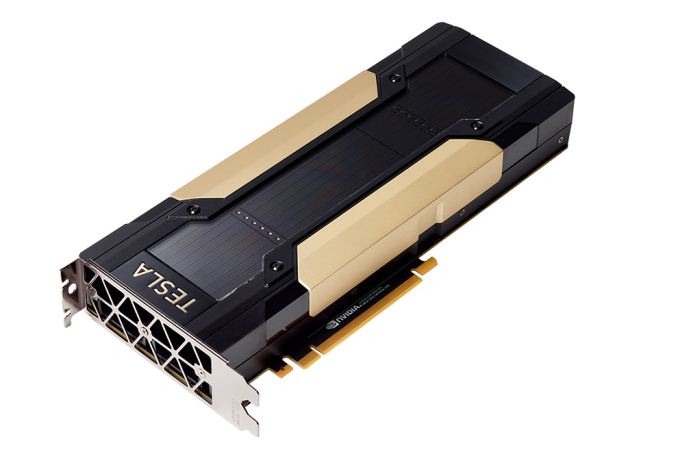
Similar to last year, at this year's International Supercomputing Conference (ISC) NVIDIA has announced and detailed a PCI Express version of their latest Tesla GPU accelerator, the Volta-based V100. The conference itself runs from June 19 to 22, and with several speakers from NVIDIA scheduled for events tomorrow, NVIDIA is set to outline its next-generation efforts in HPC and deep learning with Volta.
With Volta discussed and described at their GPU Technology Conference in mid-May, NVIDIA upped the ante in terms of both features and reticle size: V100 is 815mm2 of custom TSMC 12FFN silicon, chock full of tensor cores and unified L1 cache per SM, along with many more fundamental – and as of yet not fully revealed – microarchitectural changes.
Like the previous Pascal iteration, the Tesla V100 PCIe offers a more traditional form factor as opposed to NVIDIA’s own mezzanine-type SXM2 form factor. This allows vendors to drop Tesla cards in traditional PCIe systems, making the cards far more accessible to server builders who don't want to build around NVIDIA's SXM2 connector or carrier board. The tradeoff being that the PCIe cards have a lower 250W TDP, and they don't get NVLink, instead relying on just PCIe.
| NVIDIA Tesla Family Specification Comparison | ||||||
| Tesla V100 (SXM2) |
Tesla V100 (PCIe) |
Tesla P100 (SXM2) |
Tesla P100 (PCIe) |
|||
| CUDA Cores | 5120 | 5120 | 3584 | 3584 | ||
| Tensor Cores | 640 | 640 | N/A | N/A | ||
| Core Clock | ? | ? | 1328MHz | ? | ||
| Boost Clock(s) | 1455MHz | ~1370MHz | 1480MHz | 1300MHz | ||
| Memory Clock | 1.75Gbps HBM2 | 1.75Gbps HBM2 | 1.4Gbps HBM2 | 1.4Gbps HBM2 | ||
| Memory Bus Width | 4096-bit | 4096-bit | 4096-bit | 4096-bit | ||
| Memory Bandwidth | 900GB/sec | 900GB/sec | 720GB/sec | 720GB/sec | ||
| VRAM | 16GB | 16GB | 16GB | 16GB | ||
| L2 Cache | 6MB | 6MB | 4MB | 4MB | ||
| Half Precision | 30 TFLOPS | 28 TFLOPS | 21.2 TFLOPS | 18.7 TFLOPS | ||
| Single Precision | 15 TFLOPS | 14 TFLOPS | 10.6 TFLOPS | 9.3 TFLOPS | ||
| Double Precision | 7.5 TFLOPS (1/2 rate) |
7 TFLOPS (1/2 rate) |
5.3 TFLOPS (1/2 rate) |
4.7 TFLOPS (1/2 rate) |
||
| Tensor Performance (Deep Learning) |
120 TFLOPS | 112 TFLOPS | N/A | N/A | ||
| GPU | GV100 (815mm2) | GV100 (815mm2) | GP100 (610mm2) | GP100 (610mm2) | ||
| Transistor Count | 21B | 21B | 15.3B | 15.3B | ||
| TDP | 300W | 250W | 300W | 250W | ||
| Form Factor | Mezzanine (SXM2) | PCIe | Mezzanine (SXM2) | PCIe | ||
| Cooling | Passive | Passive | Passive | Passive | ||
| Manufacturing Process | TSMC 12nm FFN | TSMC 12nm FFN | TSMC 16nm FinFET | TSMC 16nm FinFET | ||
| Architecture | Volta | Volta | Pascal | Pascal | ||
On the surface, the addition of tensor cores is the most noticeable change. To recap, tensor cores can be liked to a series of unified ALUs that are able to multiply two 4x4 FP16 matrices together and subsequently add that product to an FP16 or FP32 4x4 matrix in a fused multiply add operation, as opposed to conventional FP32 or FP64 CUDA cores. In the end, this means that for very specific kinds (and specifically programmed) workloads, Volta can take advantage of the 100+ TFLOPS capability that NVIDIA has tossed into the mix.
As for the specific specifications of the PCIe Tesla V100, it's similarly configured to the SXM2 version, getting the same number of CUDA cores and memory capacity, however operating at a lower clockspeed in-line with its reduced 250W TDP. Based on NVIDIA's throughput figures, this puts the PCIe card's boost clock at around 1370MHz, 85MHz (~6%) slower than the SXM2 version.
Interestingly, unlike the Tesla P100 family, NVIDIA isn't offering a second-tier PCIe card based on salvaged chips; so this generation doesn't have an equivalent to the 12GB PCIe Tesla P100. NVIDIA's experience with GP100/interposer/HBM2 assembly as well as continuing production of HBM2 has likely reduced the need for memory-salvaged parts.
Finally, PCIe-based Tesla V100 accelerators are “expected to be available later this year from NVIDIA reseller partner and manufacturers,” including Hewlett Packard Enterprise, which will offer three different PCIe Volta systems.
Source: NVIDIA


27 Comments
View All Comments
bubblyboo - Tuesday, June 20, 2017 - link
Back in 2011 Intel and Nvidia settled over patents and the consequences for Nvidia was that they are pretty much NEVER going to get an x86 license or be able to make x86 emulators.http://www.anandtech.com/show/4122/intel-settles-w...
Yojimbo - Tuesday, June 20, 2017 - link
The settlement didn't grant NVIDIA any x86 license, as in it didn't force Intel to provide NVIDIA with one, but it doesn't bar Intel from granting NVIDIA an x86 license. NVIDIA won't get an x86 license because Intel doesn't want them to, not because of the settlement agreement.willis936 - Wednesday, June 21, 2017 - link
And then have a billion dollar antitrust lawsuit brought against them.andychow - Monday, September 18, 2017 - link
The earliest patents expiration for basic x86-64 implementation is 2025. They need to have legal access to things like US6877084, and that will never happen until the patent expires. They could do basic 586 type processors, but they would only be 32-bit, 2GB ram, and not run on most modern OS, which don't even support 32-bit anymore.vFunct - Tuesday, June 20, 2017 - link
Any guess on price? $10,000? $25,000?Morawka - Tuesday, June 20, 2017 - link
i'd venture to say 15k eachBateluer - Tuesday, June 20, 2017 - link
An earlier AT article on the GV100 Volta cards stated 18K/card.Ryan Smith - Tuesday, June 20, 2017 - link
Note that 18K was the effective price you were paying since you had to buy a DGX-1 to get them. It is not the stand-alone price.bill.rookard - Tuesday, June 20, 2017 - link
Folding rig anyone? Anyone? Sounds like it's got a stupid amount of processing power which is pretty darn awesome.Flunk - Tuesday, June 20, 2017 - link
Sure, have a spare $20,000/card?