Analyzing Falkor’s Microarchitecture: A Deep Dive into Qualcomm’s Centriq 2400 for Windows Server and Linux
by Ian Cutress on August 20, 2017 11:00 AM EST- Posted in
- CPUs
- Qualcomm
- Enterprise
- SoCs
- Enterprise CPUs
- ARMv8
- Centriq
- Centriq 2400
Developing a custom microarchitecture is difficult. Even with all the standards in place and licensing an instruction set such as ARM, the actual development takes time and the right people to put together, then the infrastructure to deploy at scale.
In the mobile space, we’ve seen custom cores – most notably from Apple – deviating from the regular ARM design, but also Samsung and Qualcomm are playing in that space. Qualcomm however is going one further by developing a custom core for the server and enterprise market, focusing purely on typical enterprise workloads. The current commercial ARM success in the data center comes from companies such as Cavium, who use ARM architecture licenses in a custom SoC. By developing its own high-performance core, Qualcomm is hoping to offer something different in the data center, and they’ve lifted the lid on a good chunk of the core.
The Qualcomm Centriq 2400 SoC Family, with the Falkor CPU
Back in December 2016, Qualcomm announced that it has developed its own SoC for the data center, all the while also reveaing details such as the fact that it is a custom core and that Qualcomm will be involved in the Open Compute Project (and is based on the latest version of Microsoft’s Project Olympus). We knew that Qualcomm has been aiming for a 48 core design, using ARM’s instruction set, and is aiming for the data center and enterprise markets. The goal is to carry forward knowledge of the ARM instruction set and custom core design into markets that could potentially leverage it – it also helps that the data center market has a very interesting TAM (total addressable market, in USD) of which even a small slice could reap rewards. Back in December, they were beginning to sample cloud partners and potential future customers.
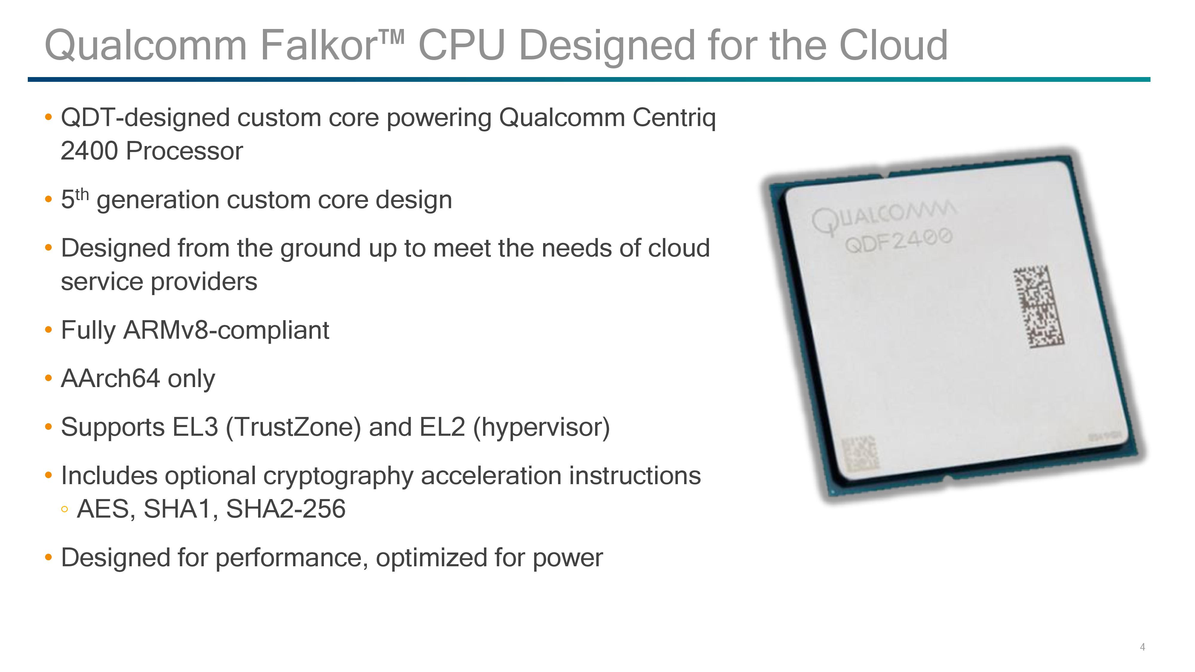
The first set of products to come out will be the Qualcomm Centriq 2400 family of SoCs. The top parts will feature 48 cores, and while today Qualcomm is ultimately communicating about said 48-core model, they have stated that the 2400-series will be a range of parts segregated by core count, performance, and power. The CPU cores, code named Falkor, will be ARMv8.0 compliant although with ARMv8.1 features, allowing software to potentially seamlessly transition from other ARM environments (or need a recompile). The Centriq 2400 family is set to be AArch64 only, without support for AArch32: Qualcomm states that this saves some power and die area, but that they primarily chose this route because the ecosystems they are targeting have already migrated to 64-bit. Qualcomm’s Chris Bergen, Senior Director of Product Management for the Centriq 2400, stated that the majority of new and upcoming companies have started off with 64-bit as their base in the data center, and not even considering 32-bit, which is a reason for the AArch64-only choice here.
The design team behind the Centriq, as explained to us, was partly formed from the custom core team from the mobile side. On the mobile side we have seen Qualcomm custom cores based on ARM’s instruction set in the form of Krait and Kryo, although this new Falkor design is not derived from either. Qualcomm states that Falkor is their 5th generation of custom CPU core design, and has been a complete ground up design specifically for the data center. The focus, we were told, was on high overall performance, high performance per watt, but also the ability to run at low power. To do this, the Centriq 2400 is set to be the first major data center design built on a 10nm process.
We already know that it will be fabbed on a 10nm process, and various media/analysts have postulated which foundry will be playing that role. Qualcomm currently has 10nm volume with Samsung through the Snapdragon 835, which is shipping in the millions. Samsung’s 10nm processes are more mature than the competition at this point, however Samsung does not have much experience with large silicon dies, tending to favor smaller SoCs due to the naturally higher yields and helping to keep fab production at a high level. The other alternative is TSMC, whose CLN10FF process was technically available for select customer orders later than Samsung, but is currently being used by Apple's A10X in the iPad Pro 2. TSMC also has experience with larger silicon, which would be of considerable benefit. Qualcomm is not announcing who their foundry partner is at this time unfortunately, although it would likely depend on relations, volume, pricing and performance.


41 Comments
View All Comments
SarahKerrigan - Sunday, August 20, 2017 - link
I seriously doubt SVE is present. As far as I know, Fujitsu is still lined up to be the first SVE user, and it's not like ultra-wide vectors are a massive boost to conventional enterprise servers.Kevin G - Sunday, August 20, 2017 - link
Using SVE requires ARM v8.2A support which this does not appear to have. The ARM v8.2A spec only was announced in January 2016, which isn't enough time to get it implemented into anything that'd be shipping now. Qualcomm could have been working behind the scenes but that would have given them perhaps another year with a spec that could change before formal publishing (i.e. may require some last minute changes right past the design would be tapping out). For a server part, that path would be unwise.SVE was announced a year ago and is far more complex than the v8.2A released due to how it handles execution width. A SVE design right now is a virtual impossibility.
Hurr Durr - Sunday, August 20, 2017 - link
I`d rather read something on x86 thing on ARM that MS and Qualcomm have than this. Much more potential for the real world.Kevin G - Sunday, August 20, 2017 - link
Can we get an editor in here?"For SoC design followers, one might look at this design and think they see similarities with designs such as AMD’s original Bulldozer design from 2011. ... Actually, after writing that last sentence, it is basically a Xeon Phi dual core module."
While perfectly readable, that last paragraph could use a bit of a rewrite due to the last sentence nullifying it. My quick stab at a rewrite:
For SoC followers, the Qualcomm pairs two modules per fabric stop similar to what Intel has implemented in their most recent Xeon Phi chips. Unlike the new grid topology in the Xeon Phi, Qualcomm is using a ring bus akin to what Intel uses on its Xeon E5 and E7 chips. Those thinking that a dual core module would follow AMD's Bulldozer philosophy will be disappointed to learn that no execution resources are shared between the cores, just the L2 cache, power management and bus interface.
The same comparisons and ideas are made but they flow to the reader a bit more logically to me.
FunBunny2 - Sunday, August 20, 2017 - link
-- Unlike the new grid topology in the Xeon Phi, Qualcomm is using a ring bus akin to what Intel uses on its Xeon E5 and E7 chips.I've long wondered how hardware engineers:
1) discover such alternatives
2) decide which one to choose
Is this fundamental math and physics laws, or trial and error? anyone know a readable (for the non-physics major, that is) source?
Kevin G - Monday, August 21, 2017 - link
Topology has been a well studied concept. At a high level, this mimics general networking design closely. The choice of on-die topology is generally at the mercy of engineering trade offs that are unique in this context.The ring bus you get an easy means of scaling the number of units but the trade of is an increase in latency around the ring bus as the numbers go up. Diminishing returns are hit as the numbers increases. With a ring though, individual units on the ring can be radically different sizes on a die as long the links between stops can be roughly the same for timing purposes. A ring bus also permits a relatively predictable latency to reach stops further away, something noteworthy for implementing coherency protocols. Another trade off with the ring design is that it'll always consume power. Nodes that are not in use still need to have the ring stop going to permit data passage through it.
Qualcomm side steps the ring issue a little bit by including two cores per ring stop, thus putting the minimum number of stops at 24. Just like Intel, I suspect on-die IO like PCIe, memory controllers etc. will have their own ring stops. It is not clear if this all on one massive ring bus or like the last generation of E5/E7 high core count chips, several rings are used with discrete bridges between them. Intel never went beyond 16 ring stops in a design.
A grid topology requires far greater engineering resources to implement correctly. Physical size has to be the same for those nodes in the middle of the grid but there is a bit of wiggle room along the perimeter to expand in one of the two dimensions (handy for things like PCIe, memory controllers that have a fixed need per socket). Cache coherency has to account for variable latency between nodes on the grid: there are several paths to between source and destination. The main benefit of a grid though is that scaling is vastly improved as core count increases. Another benefit is that not all the links in between cores needs to be active to move data. This saves power. Due to the ability to route around congested links, the individual links between grid nodes do not necessarily have to be as wide as those on a ring, saving a bit of energy there while maintaining similar aggregate bandwidth. For servers, multi-pathing of data (ie sending it twice) is also possible for increased RAS if an error in transmit is encountered along a particular path. Intel hasn't indicated that they're doing multipathing but could be a feature they add down the road. In the future if chips stacking emerges outside of research labs as feasible, the grid topology can also expand into the 3rd dimension.
The recent Xeon Phi isn't Intel's first attempt at a grid topology. The first publiclly shown off design was there Terascale research chip a decade ago. ( http://www.eetimes.com/document.asp?doc_id=1303295 ) Inter core topology was a major driver of that research effort and the recent Xeon Phi and Xeon series are the result of those efforts. Intel isn't event the first to implement a grid topology. The Compaq/DEC Alpha EV7 did so between sockets and permitted up to 64 sockets in an 8 x 8 grid from the early 2000's. IBM used a grid-like design for their BlueGene super computer designs to move data, though that wasn't cache coherent. There could be earlier instances as those are a few that I know off hand.
FunBunny2 - Monday, August 21, 2017 - link
thanks. much clearer.Ryan Smith - Sunday, August 20, 2017 - link
Thanks!Lord-Bryan - Sunday, August 20, 2017 - link
"So we have to admit that we were surprised by Qualcomm releasing so much information about the pipeline. When we’ve ever asked the mobile CPU team about Krait and Kryo, we usually hit a brick wall, left with a PR answer of a ‘custom core design’ or the guide of ‘protecting our design"Well am not surprised, releasing architectural details of server cpus, has always been an industry norm. It is something they just have to do if they want to be relevant, you can't just sell black boxes worth thousands of dollars to just anyone.
Lord-Bryan - Sunday, August 20, 2017 - link
Plus developers will have to know how the processor works in other to optimize applications for it, Qualcomm is playing with the big boys now, no room for unnecessary pride.