Intel Launches New Pentium Silver and Celeron Atom Processors: Gemini Lake is Here
by Anton Shilov on December 12, 2017 10:00 AM EST- Posted in
- CPUs
- Intel
- Atom
- SoCs
- 14nm
- Goldmont
- Gen 9
- Gemini Lake
- Goldmont Plus
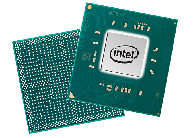
Intel on Monday introduced its next-generation Pentium Silver and Celeron platform and processors. These processors are under the codename 'Gemini Lake' and are focused on low-power platforms for inexpensive desktops and mobile computers.
The new Gemini Like SoCs feature improved CPU cores over the previous generation, an enhanced media decoding/encoding engine, and a new display pipeline. Intel promises to offer higher performance than predecessors while consuming about 6 W or 10 W, depending on the application. The higher-end Gemini Lake SKUs will be sold under the Pentium Silver brand, whereas the entry-level models will carry the Celeron name.
The Platform
Gemini Lake is Intel’s third-generation low-power SoC made using the company’s 14 nm manufacturing technology. On a high level, the Gemini Lake is an evolution of the Apollo Lake launched last year, but under the hood, there is a number of differences that seem important. The relative maturity of fabrication process would be expected to allow Intel to increase transistor budget of the new chip without decreasing yields, thus enabling higher performance and a potentially an improved feature set.
| Comparison of Intel's Entry-Level PC and Tablet Platforms | ||||||
| AnandTech.com | Bay Trail | Braswell | Apollo Lake | Gemini Lake | ||
| Microarchitecture | Silvermont | Airmont | Goldmont | Goldmont Plus | ||
| SoC CodeName (Embedded) | Valleyview | Braswell | Apollo Lake | Gemini Lake | ||
| Core Count | Up to 4 | |||||
| OOOE Architecture | 2-wide | 3-wide | ||||
| Graphics Architecture | Gen 7 | Gen8 | Gen9 | Gen9 w/Gen10 Features |
||
| EU Count | - | 16 | 12/18 | 12/18 | ||
| Multimedia Codecs |
MPEG-2 MPEG-4 AVC VC-1 WMV9 HEVC (sw) VP9 (sw) |
MPEG-2 MPEG-4 AVC VC-1 WMV9 HEVC (8-bit sw/hybd) VP9 (sw/hybd) |
MPEG-2 MPEG-4 AVC VC-1 WMV9 HEVC VP9 |
MPEG-2 MPEG-4 AVC VC-1 WMV9 HEVC HEVC 10-bit VP9 VP9 10-bit |
||
| Process | 22 nm | 14 nm | 14 nm | 14 nm | ||
| Launch | Q1 2014 | H1 2015 | H2 2016 | H1 2018 |
||
Intel’s Gemini Lake SoC is based on up to four Goldmont Plus x86 cores that feature a three-wide issue architecture and supports:
- SGX, which is required by some multimedia applications because of the latest DRM technologies,
- SHA-NI, to speeds up cryptography,
- UMIO, a security feature, and
- RDPID instruction set extensions.
The GLM+ cores inside Gemini Lake SoCs are accompanied by 4 MB of L2 cache, which we believe is a last level unified cache (Intel doesn't actually confirm this), but is double from the Apollo Lake design. The enlarged cache can positively affect performance in various applications - as a rule of thumb doubling a cache cuts the miss rate by the square root of 2 (41%) at the expense of latency and power, but we don’t expect dramatic increases in performance compared to Apollo Lake across the board. The new SoCs operate at about the same frequencies as their predecessors.
![]()
Intel says that the new Pentium Silver N5000/J5005 processors are 58-68% faster than the Pentium N3540/J2900 chips (Bay Trail platform featuring the Silvermont architecture, three generations old) in SYSMark 2014 SE. The improvement looks significant, especially keeping in mind rather high clocks of the Bayview SoCs, but is not completely surprising. The older Silvermont cores features a two-wide issue architecture, were equipped with smaller caches and featured a single-channel (64-bit) DDR3 memory controller - the new Gemini Lake platform is also more energy efficient than the Bay Trail platform introduced nearly four years ago because of architectural innovations and a thinner process technology. We yet have to test the new Gemini Lake-based products ourselves to find out real-world performance benefits brought by the enlarged cache, but at this time we have to report what Intel gives us.
Video and Memory
When it comes to graphics, the Gemini Lake uses the same iGPU as Apollo Lake but with updated features: the Gen9LP core with up to 18 EUs running at 250 – 800 MHz frequency and supporting the Direct3D Feature Level 12_1 feature set. Meanwhile, the is iGPU is outfitted with the new-generation media engine found in the Kaby Lake processors that features hardware encoding/decoding of 4K HEVC and VP9 (8-bit and 10-bit) video.
It is equipped with Intel’s Gen10 display controller supporting native HDMI 2.0 output as well as the Local Adaptive Contrast Enhancement (LACE) designed to improve visibility in glare and bright light. So, while graphics performance of Gemini Lake’s iGPU is not higher when compared to the direct predecessor, the revamped media engine, LACE support and the new display pipeline allow Intel to brand it as the UHD Graphics 600-series.
As for memory sub-system, the Gemini Lake SoCs have a 128-bit memory controller that supports DDR4 and LPDDR3/4 at up to 2400 MT/s, but no longer supports DDR3L, which is an outgoing standard anyway. We are not sure that all designs will use all the memory channels, but at least it is possible to outfit a Gemini Lake SoC with a memory sub-system offering up to 38.4 GB/s of bandwidth. Furthermore, DDR4 memory support will enable OEMs to build cheaper systems based on the Gemini Lake because DDR3L (as well as LPDDR3/4) are currently more expensive than commodity DRAM.
Storage and Connectivity
Moving on to storage and connectivity. Gemini Lake supports two conventional SATA HDDs and SSDs, PCIe 2.0 x2/x4 SSDs, as well as eMMC 5.1 storage solutions. As for I/O interfaces, the new SoCs feature USB 3.0/2.0, USB Type-C, SPI, SDXC and other modern buses.
The most import important I/O-related addition to the Gemini Lake (when compared to the Apollo Lake) is the CNVi (Connectivity Integration Architecture) MAC blocks for Wi-Fi, Bluetooth and baseband modem. The addition of the CNVi is rather important because it enables Intel’s partners among OEMs to throw in a relatively inexpensive RF module that brings support for necessary wireless connectivity standards instead of buying a more expensive adapter. Since the Gemini Lake SoCs cost exactly the same amounts of money as their predecessors, the CNVi architecture enables PC makers to cut down BOM costs for at least some of their SKUs (at least, according to Intel). Unfortunately, since Intel does not disclose pricing of its CNVi RF modules and Wi-F + BT models, we do not know how significant those BOM savings might be.
For Gemini Lake-based devices Intel proposes to use the Wireless-AC 9560 product that supports 802.11ac wave2 Wi-Fi with 160 MHz channels along with Bluetooth 5.0. The Wireless-AC 9560 supports up to up to 1.73 Gbps downlink with MU-MIMO, which is why Intel is advertising Gigabit Wi-Fi in connection with the Gemini Lake. Keep in mind that not all systems based on the Gemini Lake will use the Wireless-AC 9560 since PCIe Wi-Fi controllers are perfectly supported by the new SoCs and if an OEM has a boatload of previous-gen Wi-Fi chips, it is going to use it for their upcoming PCs.
The Family
The Gemini Lake family consists of six SKUs: two Pentium Silver models and four Celeron SoCs. The Pentium Silver chips cost $161 in 1000-unit quantities, they have higher clocks as well as all four cores enabled. The new Celerons cost $107 in commercial quantities, feature lower frequencies as well as four or two cores, depending on the model.
TDP levels of Intel’s Gemini Lake SoCs remain at 10W and 6 W, respectively. Meanwhile the SDP of the mobile-class SKUs will increase to 4.8 W (from 4 W), which is important for thinner designs. Speaking of designs, it is noteworthy that the Gemini Lake SoCs use a new flip-chip packaging (FCBGA1090) and therefore are not pin-to-pin compatible with the predecessors. The new SoC form-factor will require OEMs to make new PCBs for their Gemini Lake-based systems, and because they are a bit smaller it could save space for battery.
| Intel Gemini Lake Lineup | ||||||
| Desktop J-Series | Mobile N-Series | |||||
| Pentium Silver J5005 |
Celeron J4105 |
Celeron J4005 | Pentium Silver N5000 | Celeron N4100 | Celeron N4000 | |
| Cores | 4 | 2 | 4 | 2 | ||
| Base CPU | 1.5 GHz | 1.5 GHz | 2.0 GHz | 1.1 GHz | 1.1 GHz | 1.1 GHz |
| Turbo CPU | 2.8 GHz | 2.5 GHz | 2.7 GHz | 2.7 GHz | 2.4 GHz | 2.6 GHz |
| Cache | 4 MB | |||||
| CPU uArch | Goldmont Plus | |||||
| iGPU | UHD 605 | UHD 600 | UHD 605 | UHD 600 | ||
| iGPU EUs | 18 | 12 | 18 | 12 | ||
| iGPU Freq | 800 | 750 | 700 | 750 | 700 | 650 |
| TDP | 10 W | 6.5 W | ||||
| SDP | - | 4.8 W | ||||
| RAM | 128-bit DDR4/LPDDR3/LPDDR4 memory controller, up to 2400 MT/s, up to 8 GB |
|||||
| PCIe 2.0 | 6 Lanes | |||||
| Packaging | FCBGA1090 25×24 mm | |||||
| Tray Price | $161 | $107 | $107 | $161 | $107 | $107 |
What is noteworthy about the Gemini Lake SoCs is that CPU base frequencies have not changed compared to respective Apollo Lake SKUs and burst frequencies only increased slightly (by 200 MHz, less than 10%). Therefore, all general-purpose performance benefits that Gemini Lake may have over their immediate predecessors are going to be originated from larger caches and whatever microarchitectural optimizations the new Goldmont Plus cores may have. Certainly, new instruction set extensions will bring their benefits, but only after software starts to use them.
As for iGPU performance, do not expect Gemini Lake SoCs to offer better performance in games than their direct predecessors. Meanwhile, hardware-accelerated HEVC/VP9 media playback is a feature not to miss because of quality/smoothness and energy-efficiency improvements.
| Intel Gemini Lake vs Apollo Lake | ||
| Desktop | Gemini Lake: Pentium Silver J5005 |
Apollo Lake: Pentium J4205 |
| uArch | Goldmont+ | Goldmont |
| Cores | 4 | 4 |
| Base CPU | 1.5 GHz | 1.5 GHz |
| Turbo CPU | 2.8 GHz | 2.6 GHz |
| Cache | 4 MB | 2 MB |
| iGPU | UHD 605 | UHD 505 |
| EUs | 18 | 18 |
| Turbo iGPU | 800 MHz | 800 MHz |
| TDP | 10W | |
TDP levels of Intel’s Gemini Lake SoCs for desktops and mobile PCs (including notebooks, tablets, etc.) have not changed and remain at 10W and 6 W, respectively. Meanwhile, SDP of mobile SKUs will increase to 4.8 W (from 4 W), which is going to be important for thinner designs.
Speaking of designs, it is noteworthy that the Gemini Lake SoCs use the new FCBGA1090 package and therefore are not pin-to-pin compatible with the predecessors. The new package measures 25×24 mm and is smaller than the FCBGA1296 package used for the Apollo Lake SoCs (which measure 24×31 mm). The new SoC form-factor will enable OEMs to make PCBs for their Gemini Lake-based systems a bit smaller and save space for battery. Furthermore, it is logical to expect Intel to encourage PC makers to use BGA SSDs as well as eMMC storage devices with their Gemini Lake-based offerings to make them sleeker and/or install a bigger accumulator to provide a longer battery life.
The Gemini Lake platform has existed in Intel’s public plans for quite some time and the chipmaker’s platforms started to show it in their roadmaps in the middle of the year. Most of Gemini Lake-based products were slated to ship in 2018, so the formal announcement in mid-December, three weeks before OEMs show their designs at CES, comes as a surprise. Intel does not usually announce its low-power platforms for inexpensive desktops, AIOs, notebooks, 2-in-1s and tablets with fanfares, but this time Intel’s announcement can be considered as a very quiet one. Perhaps, Intel does not want to steal the thunder from its partners, or there are other reasons. But the bottom line is the company is not sharing many details and getting information about the Gemini Lake in general at this time. Perhaps, there will be more data to process at CES.
Intel anticipates the first Gemini Lake products to arrive in the first quarter of 2018, so expect major OEMs to show their Gemini Lake-based devices at CES next month and make them available a bit later.
Source: Intel
Additional 12/13:
After a few back and forth emails with Intel, we can confirm that the Gemini Lake family is built on 14nm, rather than 14+ or 14++ which are newer variations of Intel's 14nm process technologies. Intel also confirmed the microarchitecture is a three-wide decode, the same as Goldmont, with the following execution port layout:
There are three integer ALUs, one jump port, one load port, one store port, and two general purpose FP/vector ports, so we can dispatch up to 8 instructions in a single cycle.
We're requesting more information.


56 Comments
View All Comments
iwod - Wednesday, December 13, 2017 - link
I just looked it up and the 10W seems to have performance of a single core Sandy Bridge and much faster Multi Core in Geekbench.HEVC 10Bit Support.
Since Metal 2 is supported on Gen9 iGPU, i am guessing this is going to be the chip for next Mac Mini?
peevee - Wednesday, December 13, 2017 - link
14nm vs 14nm, 4 cores vs 4 cores, 3 issue vs 3 issue, 1.5GHz vs 1.5GHz, 12/18 Gen 9 vs 12/18 Gen 9... So basically the same thing as Apollo Lake. Brand engineering.mode_13h - Friday, December 15, 2017 - link
The CPU has double the L2 cache and new instructions (including SHA acceleration). I had read that it was supposed to be 4-way issue, but I guess it's not.The GPU has 10-bit support for HEVC & VP9 and native HDMI 2.0.
The SoC also has built-in AC wireless.
So, think of it as more of a mid-generation refresh, rather than either a tick or a tock. IMO, the clock speed & cache size improvements are worth something. The cache size will be especially helpful for implementations with single-channel memmory, which are all too common, sadly (recall that integrated graphics likes memory bandwidth).
raywzou8 - Wednesday, April 11, 2018 - link
Does anyone have first hand experience if 2x 8gb stick of ram will work on nuc7pjyh, or an asrock board with either j4005, j4105, or j5005Jorgp2 - Tuesday, October 30, 2018 - link
This is a really late reply.But i have been running a 4GB + 8G; for a while now, i don't see why 8+8 wouldnt work