MediaTek Announces New Premium Helio P60 SoC
by Andrei Frumusanu on March 1, 2018 9:30 AM EST- Posted in
- Smartphones
- Arm
- Mobile
- Trade Shows
- MediaTek
- Mali
- Helio
- MWC 2018
- P60
- A73
- A53
- ARM Cortex
BARCELONA, ESP – Earlier this week MediaTek announced a new entry in the Helio SoC line-up, the Helio P60. The P60 comes with a strategy change for MediaTek as the company is doubling down on the super-midrange “premium” category and expanding that range into multiple sub-tiers.
The strategy change comes from market and lack of success in the high-end Helio X series. Last year’s Helio X30 had only a few design wins and was relatively late to market. MediaTek seems to have had a string of bad luck with the X20 and X30 as both came on either problematic or very delayed manufacturing process nodes which lost them important design wins. As more vendors switch over to custom designs in the high-end and Qualcomm puts more pressure with competitive designs, MediaTek decided to put a hold on the X series for now and concentrate in the range where it is very successful, the P series.
The this new segmentation means that the P60 doesn’t position itself as direct successor to late last year’s P23 and P30 but rather as a tier above them, hence the naming scheme.
| MediaTek Current P-Series | |||
| SoC | Helio P23 | Helio P30 | Helio P60 |
| CPU | 4x Cortex A53 @ 2.3GHz 4x Cortex A53 @ 1.65GHz |
4x Cortex A53 @ 2.3GHz 4x Cortex A53 @ 1.65GHz |
4x Cortex A73 @ 2.0GHz 4x Cortex A53 @ 2.0GHz |
| GPU | Mali G71MP2 @ 770MHz | Mali G71MP2 @ 900MHz | Mali G72MP3 @ 800MHz |
| APU / NPU / AI Proc. / Neural IP | - | 2x 140GMACs | |
| Memory | 1x 32bit LPDDR3 @ 933MHz 2x 16bit LPDDR4X @1500MHz |
2x 16bit LPDDR4X @ 1600MHz | 1x 32bit LPDDR3 @ 933MHz 2x 16bit LPDDR4X @ 1800MHz |
| ISP/Camera | 1x 24MP or 2x 13MP | 1x 25 MP or 2x 16MP | 1x 32MP or 2x 20+16MP |
| Encode/ Decode |
2160p30 H.264 | 2160p30 H.264 & HEVC | 2160p30 H.264 & HEVC |
| Integrated Modem | Category 6 DL = 300Mbps 3x20MHz CA, 64-QAM UL = 50Mbps 64-QAM |
Category 7/13 DL = 300Mbps 3x20MHz CA, 64-QAM UL = 150Mbps 2x20MHz CA,64-QAM |
Category 7/13 DL = 300Mbps 3x20MHz CA, 64-QAM UL = 150Mbps 2x20MHz CA,64-QAM |
| Mfc. Process | 16FFC | 16FFC | 12FFC |
The P60 is the first SoC in the P-lineup to employ “big” microarchitecture cores as it uses 4x Cortex A73 cores at up to 2.0GHz – a significant performance boost in performance over the P23 and P30’s A53 cores. The efficiency cores are naturally still Cortex A53’s and they run at the same 2.0GHz frequency as the performance cluster.
On the GPU side we see an update in the IP as MediaTek in turn transitions from G71 to G72. The P60 uses a G72MP3 running at up to 800MHz and promises a 25% gaming efficiency boost (at up to 70% higher GPU performance).
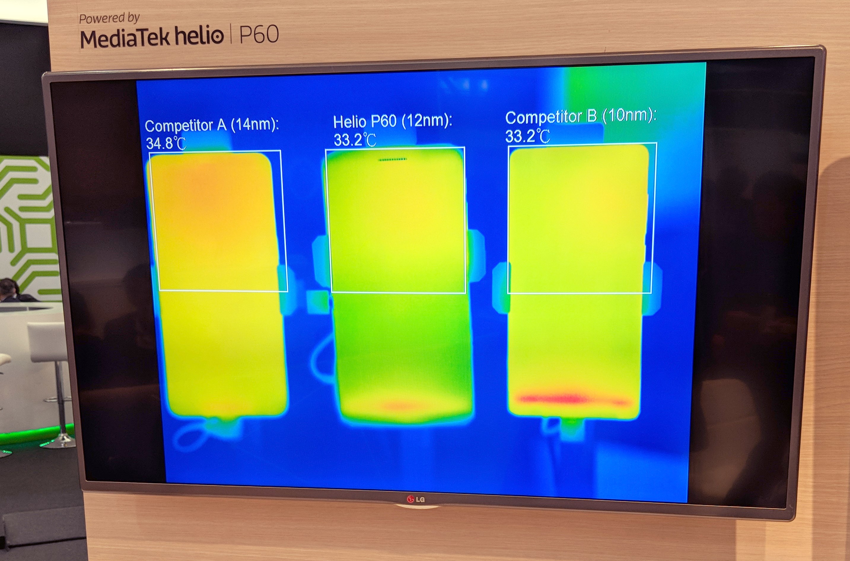
Snapdragon 660 vs Helio P60 vs Snapdragon 835 Thermal Comparison @ MWC2018
The P60 is the first mobile SoC to come manufactured on TSMC’s new 12nm 12FFC process node. 12FFC is a shrink of 16FFC and uses the same tools – it’s a cost effective alternative to the more expensive 10FF process which requires quad-patterning. While 12FFC does not quite achieve the die size reduction that 10FF would, it’s extremely competitive in terms of power characteristics and reaches near the same efficiency. I asked MediaTek about the company process roadmap plan and they will focus exclusively on 12FFC for 2018 and have no plans for further 10nm silicon. The next generation will jump directly to 7nm in mid 2019 (after other vendors) when mass production will have reached mature and cost-effective levels.
The P60 is the first SoC to bring dedicated neural network accelerators into the mid-range. MediaTek’s denomination for such IP is APU (AI Processing Unit) so that’s yet another term added to the varied basket of abbreviations from different companies. MediaTek wouldn’t disclose the IP provider but say’s it’s a dual-core implementation offering 2x140GMACs. MediaTek will offer a custom software stack called NeuroPilot which will be compatible with Google’s NN API and frameworks such as TensorFlow, TF Lite, Caffe and Caffe2.
The modem subsystem remains the same as on the Helio P30 – it supports LTE up to Category 7 with 3x20MHz CA and 300Mbps download speeds and Category 13 with 2x20MHz CA for up to 150Mbps upload speeds.
The Helio P60 is in production now and we should see consumer smartphones with the chipset available starting early Q2 2018.


74 Comments
View All Comments
jjj - Friday, March 2, 2018 - link
I'm nobody's fan and I take any such suggestion as an insult but that wasn't your intention so i'm not gonna get upset here. Anyway. A75 would offer the possibility of much higher peak perf vs A73. They could go as high as SD845 and Qualcomm would be reluctant to follow with SD670. A73 at 2.5GHz should be behind A75 at 2GHz, at least in FP as that's where A73 is weak so , depending on everything else the SoC offers, they might have to price it significantly lower while also winning far fewer sockets.35-40$ is a lot, even the very high end would be lower if there was competition.What you want (assuming you want a tiny MP2), would be nice at 12-15$ next year on 7nm, with a newer core, not A75.
Cost wise, 7nm does not need EUV to be much cheaper than 14/16nm and EUV won't do a lot on the cost side. EUV arrives when it arrives and then folks struggle to avoid double patterning, then maybe high-NA EUV arrives on schedule in 2024 , or maybe not... EUV is too late to provide a huge upside, it will help and it is needed but there is revolution on the cost side.
As for a focus on reasonable solutions, that's what MTK has been mostly doing and they got screwed by marketing because consumers are less than reasonable. What they need is to beat Qualcomm on the GPU side, consistently., at any cost. Aside being aggressive and flawless execution but that's a given.
jjj - Friday, March 2, 2018 - link
there is NO revolution*ZolaIII - Saturday, March 3, 2018 - link
& revolution eats it's children. Development of the Chinese home grown full complex semiconductor manufacturing won't be a revolution but an overtaking & US is aware of it.serendip - Friday, March 2, 2018 - link
EUV will take a long time to reach commercial production so we could be stuck with 10-12nm for a while.The only way to beat Qualcomm right now is to have a SoC that's equal on the CPU side with equal or better GPU performance, along with a decent modem. HiSilicon and Samsung have come close for the high end but Mediatek are behind in the flagship, midrange and low end segments. In other words, they're way behind. A DynamIQ A75+A55 chip for the midrange priced lower than the SD670 would make Mediatek more attractive to OEMs.
ZolaIII - Saturday, March 3, 2018 - link
It's not possible to beat QC on the flagship segment regarding the GPU. On the higher end mid range segment it's probably possible to match it & most folks would be satisfied with what. EUV is apparently hire already.ZolaIII - Saturday, March 3, 2018 - link
Their is no much use of clocking either A73 or A75 beyond the 2 GHz point & even so only for a burst tasks over 1.6GHz with FinFET and 1.2GHz with bulk planar or FD-SOI they begin to leak as hell. Over 2 GHz the power consumption rises almost exponentially.You didn't read right; the GT8540 is a flag Imagination last generation GPU with four clusters so it's huge that's why I told 35~40$ as PowerVR cluster is actually bigger than MALI cluster. The MP2 whose for Tensilica P6 Vision DSP.
Cost wise increased complexity along with a double or triple pattering now dose add significantly to the price as the wait period between patterns is long, wafers are stored in sterile environment between them and it significantly reduces output per time unit. EUV is there for significantly reducing that wait so it will boost the output & lower the cost. As much as I did read recently Samsung already implemented it on it's 7nm FinFET, it's production ready & production is starting (already or soon). Anyway products on it are coming 1Q next year. I know EUV is not preliminary needed at 7nm but it will be a game changer as you will see. Other than that 7nm isn't cheaper than previous nodes as it also employees use of rare earth conduct materials but that doesn't actually rise the final price all that much. To simplify things if you get 50% more cells (7 vs 10nm)on 300mm wafer but you also need 50% more time to produce it then the cost is the same, if you need only 75% of time (EUV) than the cost is slashed in half.
MTK or even Nv can't beat QC on performance/W, performance per square mm. What they could do is beat it at the higher midrange segment by employing bigger GPU on more economic lithography so that it narrows the current Adreno advantages. I suggested PowerVR as it's the most competitive one known & with it they could even win. Still MTK does change less (or at least we assume so) per equal size SoC than QC (all do I am sceptic about that as QC doesn't make much money out of SoC's) if they use 30~40% cheaper lithography that gives them opportunity to put 2x sized GPU & offer it by competitive (to QC) prices (not cheaper). Up to date MTK did quite opposite to this. At the end 35~40 $ is a lot more than 15~20 $ but it doesn't make much difference on the 200~350$ product.
ZolaIII - Saturday, March 3, 2018 - link
MTK does charge less *jjj - Saturday, March 3, 2018 - link
"Can't beat" is not a realistic statement in semiconductors, they just need need to figure out how.On EUV you are not informed, at all. EUV will be inserted when, at the very least it doesn't increase costs while shortening cycle time. In Samsung's case, they might do it at any cost, even at huge losses and remains to be seen when as they have been rather silent lately on timing. The insertion is being forced and the upside will be none to minimal at first. 1 year later, 5nm arrives and it's another struggle that only gets worse with 3nm and beyond. EUV should help mitigate the escalating costs and that's a slightly optimistic scenario, it won't enable any kind of return to solid cost scaling though.
7nm DUV should offer maybe 30% savings over 14/16nm on the silicon side, dev costs are another matter. Dev costs are why folks do not migrate, high ASPs and/or vols are needed for enough total revenue, otherwise cost per transistor is lower.
ZolaIII - Saturday, March 3, 2018 - link
If someone runs twice as fast as you, you can race him but you won't win (MALI vs Adreno). If someone is 33% faster than you but you can compensate that by going to a league down you still can be a champion in that league as long as you're expenses are competitive (PowerVR on cheaper manufacturing node).I am sorry my bad I ment DUV.
As much as I can recall you ware not exactly for 22nm FD-SOI. Did this change recently? I still see it as competitive to the 12 nm FinFET on digital space while being a sure thing in RF and mixed A/D. As its easier to do things on one node only it wins overlay. They are gaining a lot of traction; for instance P6 Vision DSP whose already rooted on it, the RF part's are emerging with high speed & they have both SRAM and MRAM cell's ready for quite some time now, unfortunately wafer availability isn't good but we see that trend now globally regarding water protection & estimated prices jump. I see it as the best solution if you want to go cost effective way & you are relatively small or medium vendor especially if you are on the go for time to market.
ZolaIII - Saturday, March 3, 2018 - link
Regarding wafer production & estimated price jump *Actuality confirmed price jump.