The NVIDIA Titan V Deep Learning Deep Dive: It's All About The Tensor Cores
by Nate Oh on July 3, 2018 10:15 AM ESTA Shallow Dive Into Tensor Cores
Of the several mysteries around Volta’s mixed precision tensor cores, one of the more nagging ones was the capability of 4 x 4 matrix multiplication. To recap, the tensor core is a new type of processing core that performs a type of specialized matrix math, suitable for deep learning and certain types of HPC. Tensor cores perform a fused multiply add, where two 4 x 4 FP16 matrices are multiplied and then the result added to a 4 x 4 FP16 or FP32 matrix. The result is a 4 x 4 FP16 or FP32 matrix; NVIDIA refers to tensor cores as performing mixed precision math, because the inputted matrices are in half precision but the product can be in full precision. As it so happens, the math that tensor cores do is commonly found in deep learning training and inferencing.
And if this sounds familiar to a normal GPU ALU pipeline, then it should. Tensor cores, while being brand-new to the GPU space, are not all that far removed from standard ALU pipelines. The density has changed – they're now operating on sizable matricies instead of SIMD-packed scalar values – but the math has not. At the end of the day there's a relatively straightforward tradeoff here between flexibility (tensor cores would be terrible at scalar operations) and throughput, as tensor cores can pack many more operations into the same die area since they are so rigid and require a fraction of the controlling logic when that cost is divided up per ALU.
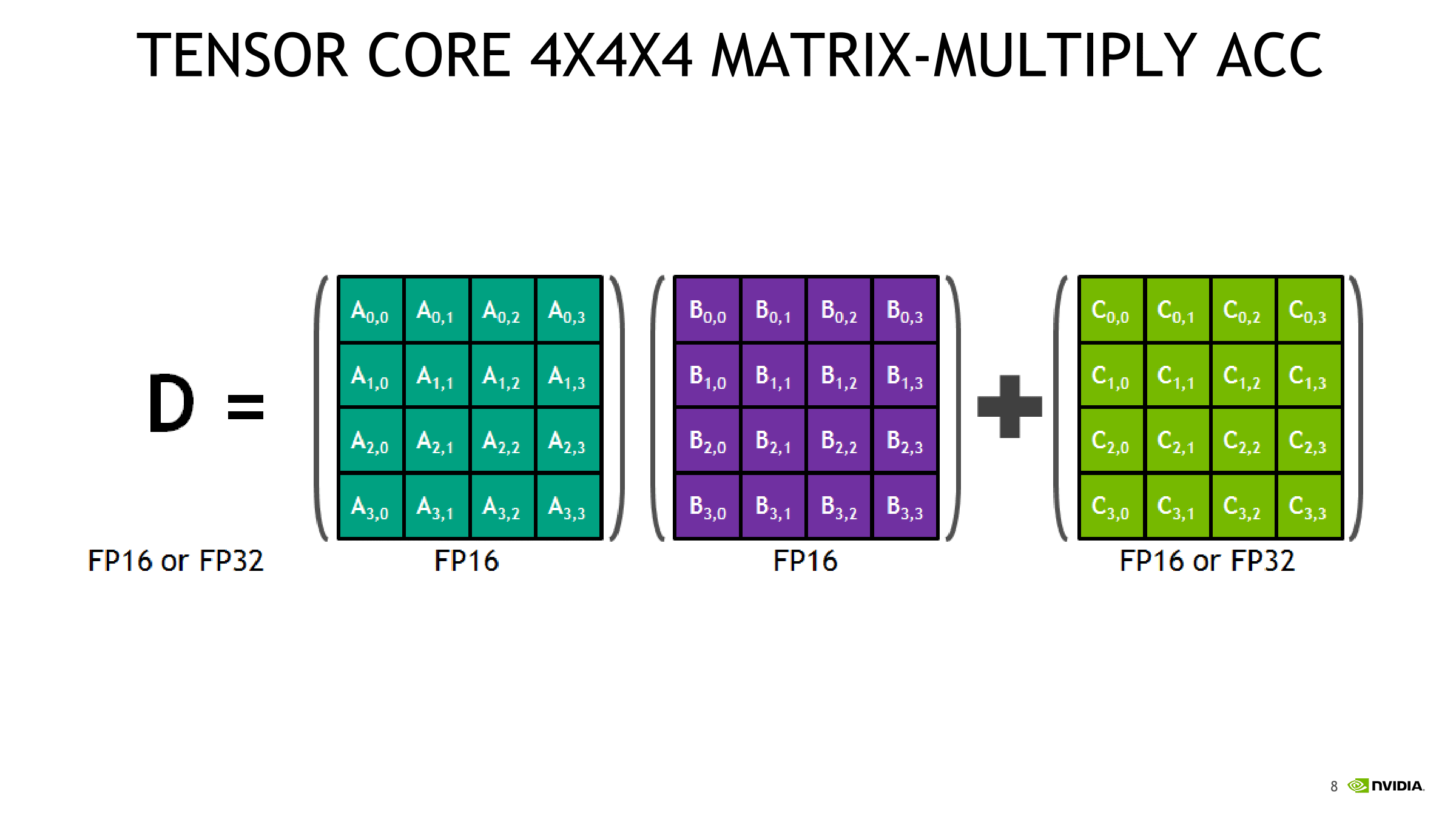
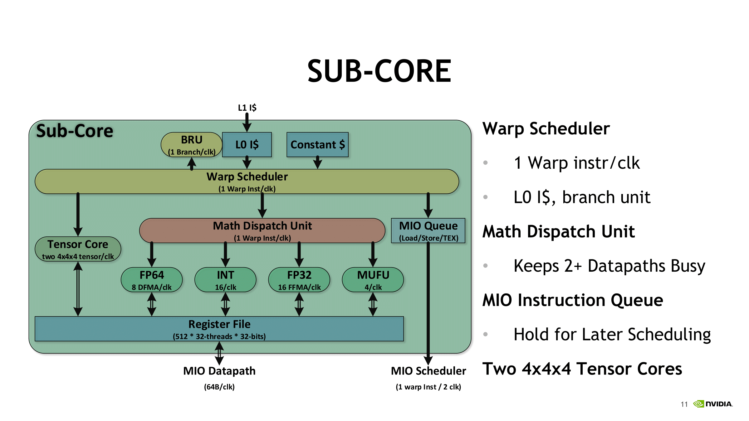
Consequently, while somewhat programmable, tensor cores are stuck to these types of 4 x 4 matrix multiplication-accumulation – and it’s not clear how and when the accumulation step occurs. Despite being described as doing 4 x 4 matrix math, in practice, tensor core operations always seem to be working with 16 x 16 matrices, with operations being handled across two tensor cores at a time. It appears that a lot of it has to do with the other changes in Volta, and more specifically, how these tensor cores are placed in an SM. For Volta, SMs were partitioned into four processing blocks, or sub-cores.
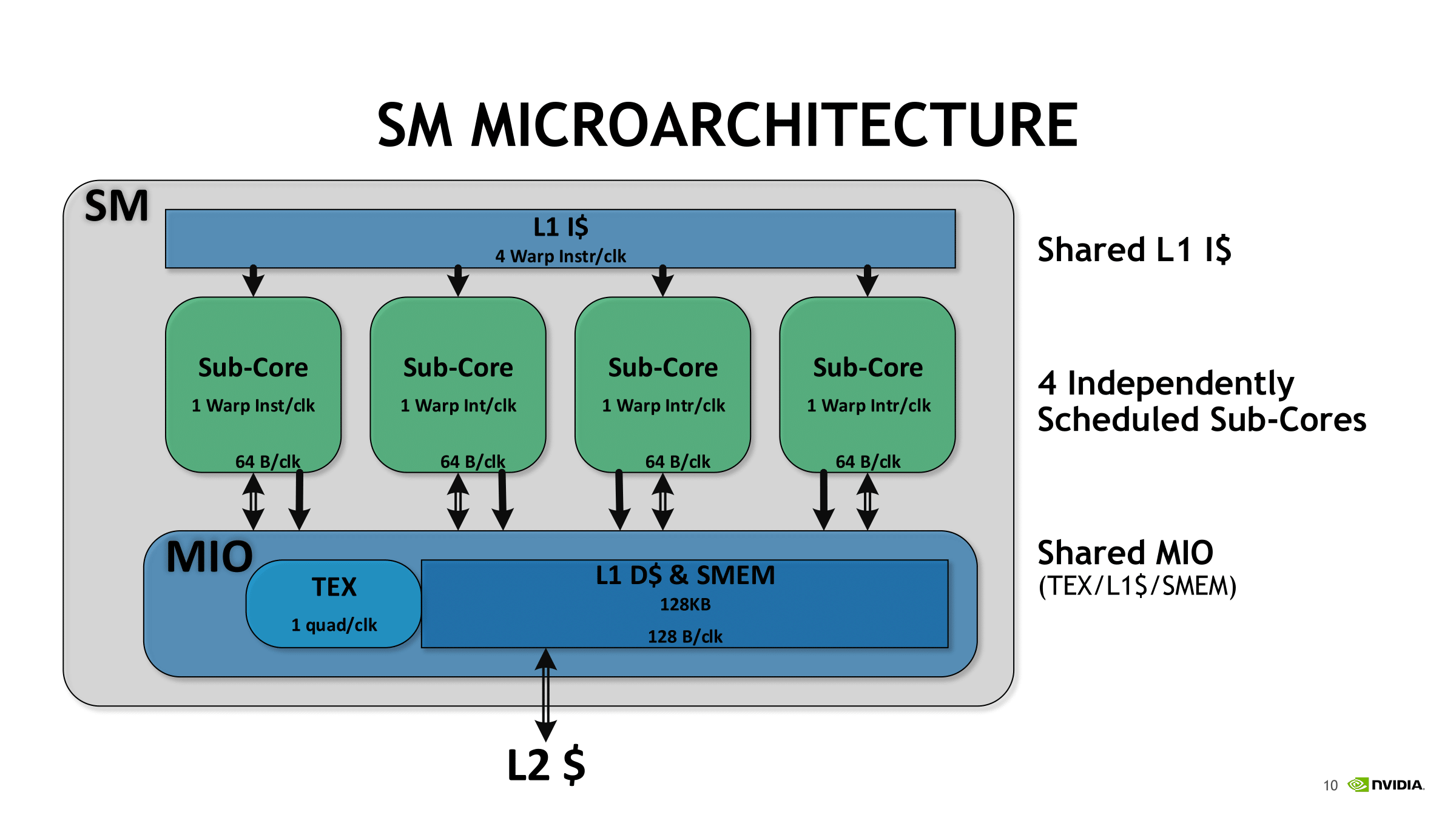
For each sub-core, the scheduler issues one warp instruction per clock to the local branch unit (BRU), the tensor core array, math dispatch unit, or shared MIO unit. For one, this precludes issuing a combination of tensor core operations and other math simultaneously. In utilizing the two tensor cores, the warp scheduler issues matrix multiply operations directly, and after receiving the input matrices from the register, perform 4 x 4 x 4 matrix multiplies. Once the full matrix multiply is completed, the tensor cores write the resulting matrix back into the register.
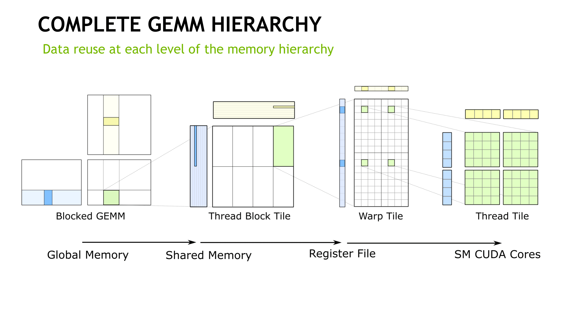
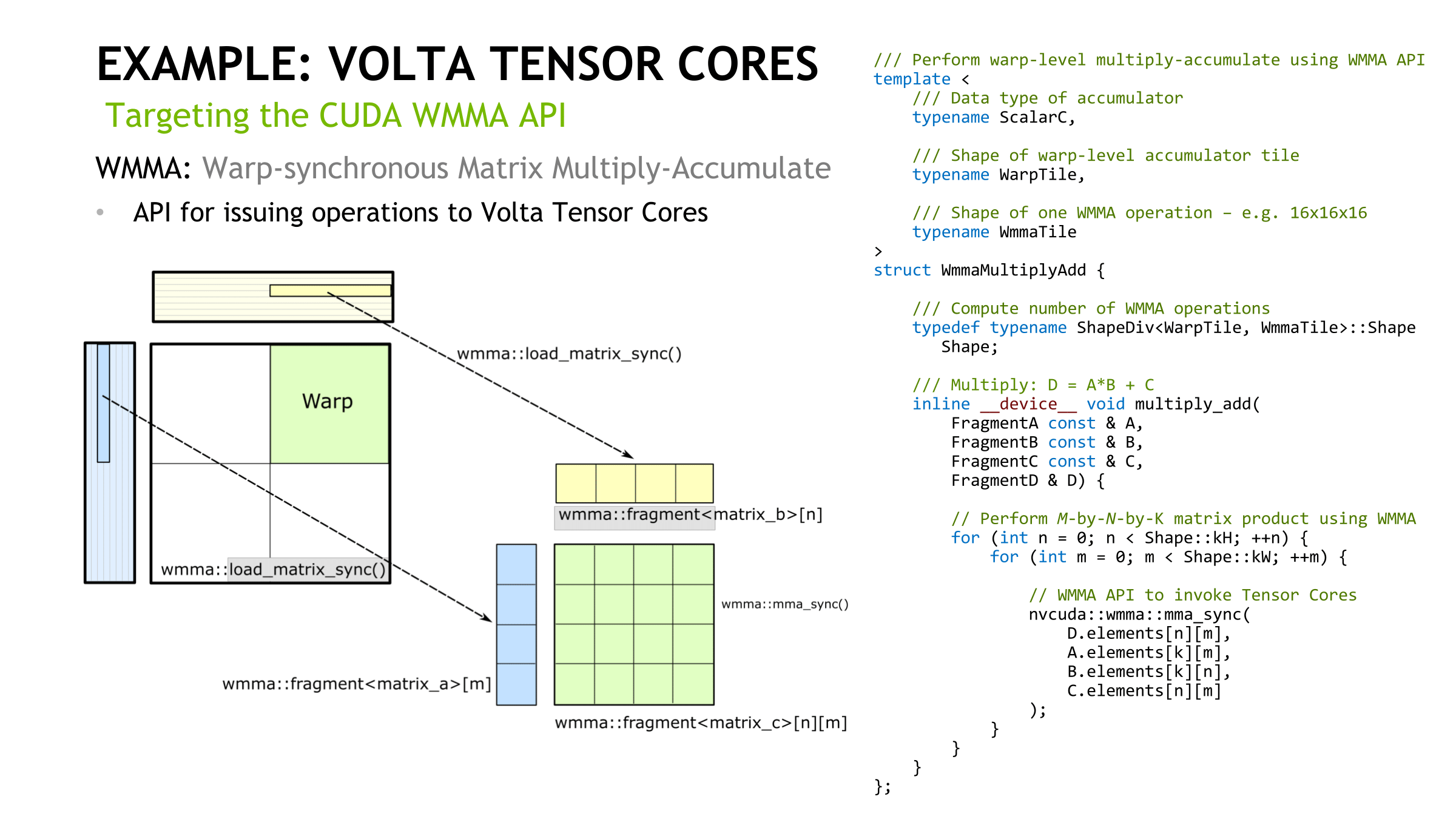
Looking at how tensor cores execute the actual instruction, opcode HMMA, only seems to raise more questions. Even at the compiler level with NVVM IR (LLVM), there are only intrinsics for warp-level matrix operations, rather than tensor cores, and warp-level remains the only level with CUDA C++ and the PTX ISA. Loading the input matrices is in the form of each warp thread holding a fragment, whose distribution and identity is unspecified. So broadly-speaking, it follows the same pattern of thread-level tiling-based GEMM computation for standard CUDA cores, and we'll circle back on that with NVIDIA's CUTLASS library in a moment.
In general terms, though, given the A*B+C tensor core operation, fragments consist of 8 FP16x2 elements (i.e. 16 FP16 elements) for A and another 8 FP16x2 elements for B, as well as 4 FP16x2 elements for an FP16 accumulator or 8 FP32 elements for an FP32 accumulator.

After the matrix multiply-accumulate operation, the result is spread out in fragments in the destination registers of each thread. Requiring warp-wide unity, these low-level operations essentially fail if one of the warp threads had exited.
Low-level microbenchmarking by a team at Citadel LLC revealed a number of Volta microarchitecture details, including tensor core operations and the fragments involved, both locations in the register and identity compared to the input matrices. They observed that a sub-core proceeds to calculate the matrix-multiply in a particular patchwork pattern, with all 32 threads of the warp in action. Conceptually, the tensor cores operate on 4 x 4 submatrices to calculate the larger 16 x 16 matrix, involving Volta’s cooperative groups and new scheduling model.
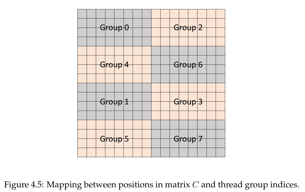
With the warp threads separated out into 8 thread groups of 4 threads, each thread group computed an 8x4 chunk serially, going through a process of 4 sets. So altogether, each thread group dealt with 1/8 of the resultant matrix.

Within a set were four HMMA steps that could be done in parallel, each applying to a 4x2 subchunk. The four threads were directly linked to those matrix values in the register, so that a single Step 0 HMMA instruction could be processed by the thread group to compute the subchunk in one go.

As matrix multiplication mathematically requires reuse of certain columns and rows, to permit parallel execution across all 8x4 chunk each 4 x 4 matrix is mapped to the registers of two threads. If applicable, the accumulate step sums the product with a stored accumulator; in this case of 4 x 4 submatrix operations to calculate a 16 x 16 parent matrix, this would include summing the sets as they were computed serially to form the corresponding chunk of 4 x 8 elements in the 16 x 16 matrix. Though untested by Citadel, it has been observed that FP16 HMMA instructions result in 2 steps rather than 4, relating to the smaller register space that FP16 occupies, and presumably a similar principle applies. Assuming that the sub-core was configured for peak output, it’s still hard to estimate without numbers, though it seems like ‘FMA ops per cycle’ is in reference to the matrices’ constituent values.
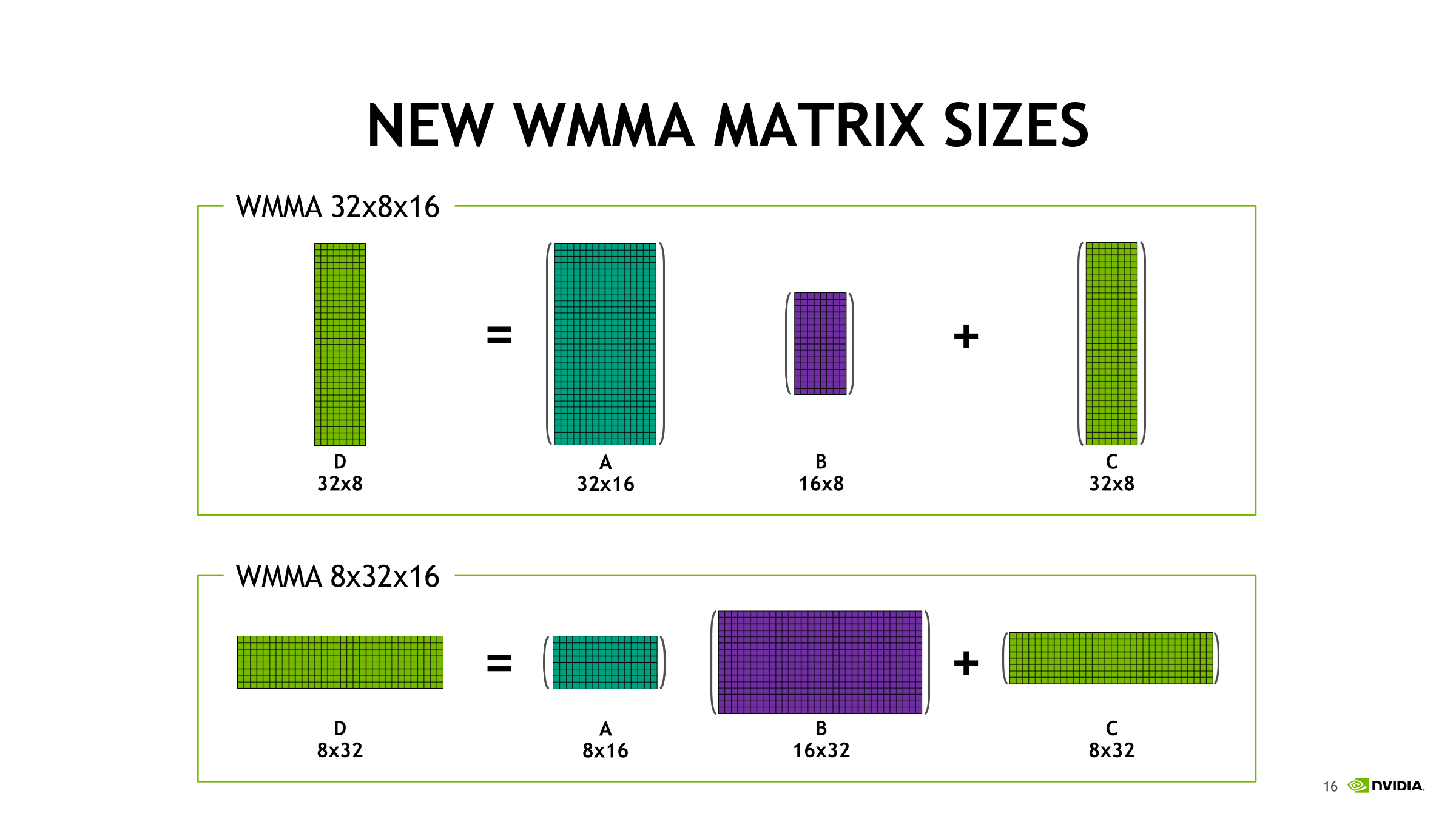
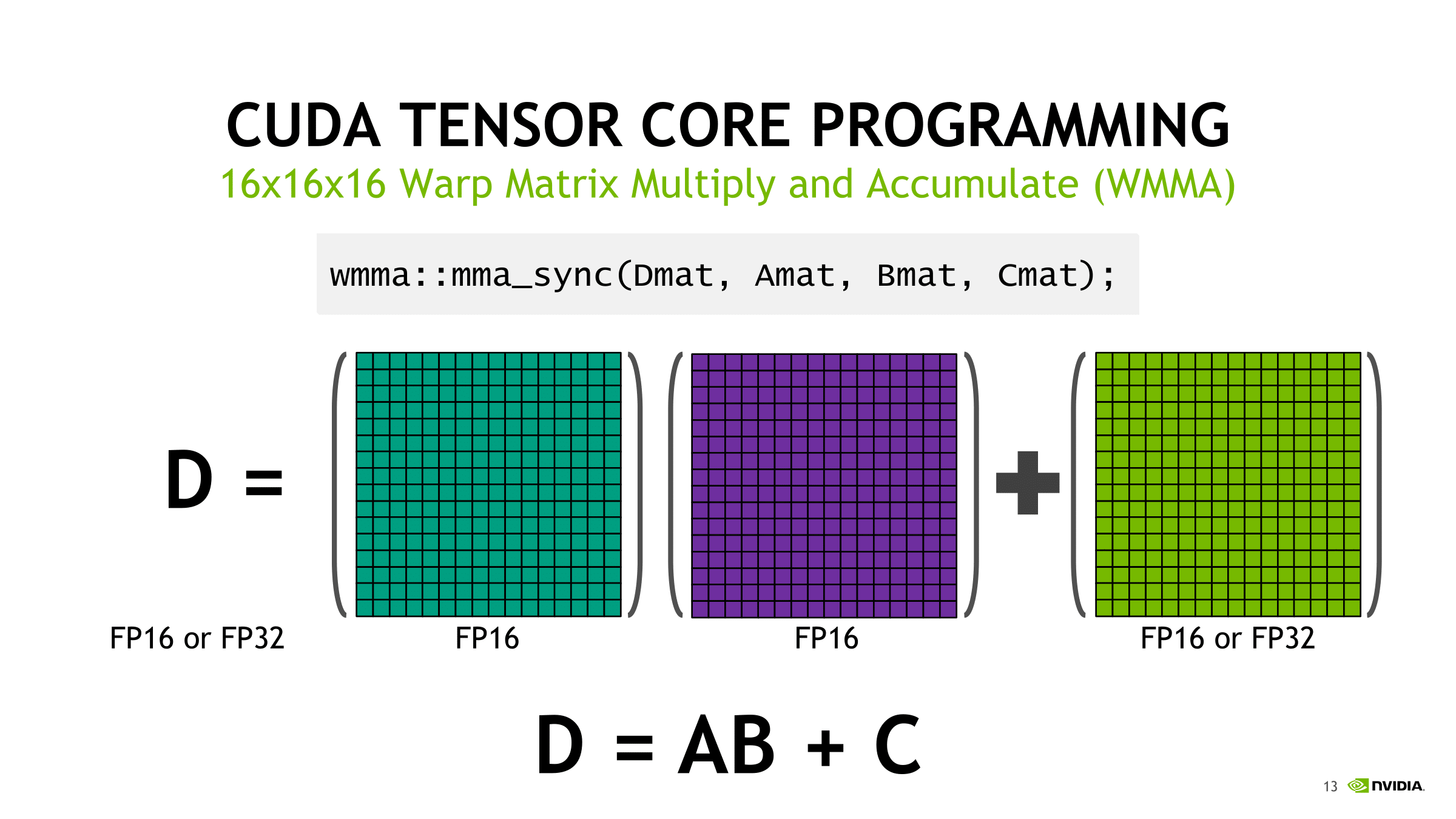
With independent thread scheduling and execution, as well as warp synchronization and warp-wide result distribution, the basic 4 x 4 x 4 tensor core operations translate into semi-programmable 16 x 16 x 16 mixed precision matrix multiply-accumulation, though with CUDA 9.1, 32 x 8 x 16 and 8 x 32 x 16 configurations are supported. For both new shapes, the multiplied matrices need the appropriate corresponding columns and rows of 16, with the end matrix being 32 x 8 or 8 x 32; this more-or-less suggests that standalone 4 x 4 x 4 matrix multiply-accumulate operations can’t be easily supported. Hard-coded warp-level behavior of register fragments, implementation of the MMA instruction, or tensor core ALUs could easily result in solely warp-level tensor core matrix math. And from a practical viewpoint, power consumption would suffer due to the increased register file usage while not significantly adding to deep learning performance.
How tensor cores operate seem to be a hardware implemented step of NVIDIA's GEMM computation hierarchy, as seen in CUTLASS, their CUDA C++ template library for GEMM operations. With traditional CUDA cores, the last step requires breaking down (i.e. 'decomposing') the warp tile structure into scalar and vector elements owned by individual threads. With the WMMA API, which right now means tensor cores, all that is abstracted away, leaving only the warp-cooperative matrix fragment load/store and multiply-accumulate to deal with. The accumulation occurs in-place as an FMA-type operation.
On the register level, NVIDIA themselves mentioned in their Hot Chips 2017 paper that “with three relatively small 4x4 matrices of multiply and accumulator data, 64 multiply-add operations can be performed.” And the per-thread program counter of the enhanced Volta SIMT model, something that enables tensor cores, usually requires 2 register slots per thread according to the whitepaper. There also may have been a change to the register structure; a 2-bank 64-bit configuration was reported by Citadel, though NVIDIA themselves have documented 4-bank 32-bit. The HMMA instructions themselves feature as much register reuse as possible, despite the other Volta enhancements (that we’ll touch on in a moment), so I can’t imagine registers aren’t bottlenecking tensor cores for the majority of cases.
For standalone 4 x 4 matrix multiply-accumulate, I suspect that the tensor core array was not physically designed for it in terms of registers, data paths, and scheduling, such that it is only useable with specific submatrix multiplications (though admittedly I’ve not studied linear algebra in some time).
In any case, from NVIDIA’s point-of-view, Volta isn’t a deep learning ASIC; it is still covering the GPGPU space, and so keeping to CUDA programmable tensor cores for applicability to GEMM/cuBLAS and HPC is only logical. With CUTLASS for CUDA C++, this is even more the case, as its WMMA API support is aimed at enabling tensor core GEMM operations for a broad range of applications. Fundamentally, the development of NVIDIA's deep learning hardware acceleration has much to do with the development of cuDNN (and cuBLAS, to a lesser extent) over the years.
-01_thumb.png)
-02_thumb.png)
-03_thumb.png)
-04_thumb.png)
-05_thumb.png)
-06_thumb.png)


65 Comments
View All Comments
SirPerro - Thursday, July 5, 2018 - link
The fancy girls with the macbook in starbucks are not exactly the target demographics for a deep learning desktop card. Or if they are, their laptop plays no part in that.This card is meant for professionals who can spend more than its price in google cloud training neural networks. For everyone else it makes absolutely no sense.
tipoo - Tuesday, July 3, 2018 - link
That Vega 56/64 in the iMac Pro pitched for deep learning also looks pretty underwhelming...Demiurge - Wednesday, July 4, 2018 - link
First of all, who "pitched" a iMac Pro for Deep Learning? Why would Apple put a $3k GPU in a model that is typically selling for $4-5k?Second, what model are you training on Vega that isn't sufficient with 2-4x the FP16/FP8/INT8 throughput of a 1080 Ti? How is that underwhelming?
mode_13h - Wednesday, July 4, 2018 - link
The GP102 in the 1080 Ti and Titan Xp doesn't support double-rate fp16. Just 4x int8 dot product, AFAIK, which you can't really use for training.Demiurge - Friday, July 6, 2018 - link
My point exactly since Vega does support double-rate FP16, among other things that the consumer GPU's typically don't support.As for the DP4A instruction, it is very much used in training.
INT8 datatype support is becoming more important, as is FP8 for reducing training time. Two more features Vega supports free of additional charge.
mode_13h - Friday, July 6, 2018 - link
If 8-bit int were acceptable for training, then why would anyone bother with fp16?Vega 10 doesn't have meaningful packed 8-bit support of any kind. It has only a couple such instructions that are intended for video compression. Vega 20 will change that, even adding support for packed 4-bit. But your comment seems oriented towards the current Vega.
Demiurge - Sunday, July 8, 2018 - link
Here's some reading (read the first line of the conclusion of the paper: Dettmers, 8-Bit Approximations for Parallelism in Deep Learning, ICLR 2016 https://arxiv.org/pdf/1511.04561.pdf):https://www.xilinx.com/support/documentation/white...
We shall disagree on "Vega 10 does not have meaningful packed 8-bit support". I'll let someone else argue with you, but I know what you mean. I don't agree, but I think I understand where you are coming from.
mode_13h - Monday, July 9, 2018 - link
Aww... don't pick a fight, then walk away!Here's the current Vega ISA doc. The only 8-bit packed arithmetic I see is unweighted blending and sum of absolute differences. AFAIK, this is not a useful degree of functionality for deep learning. If I'm wrong, show me.
http://developer.amd.com/wordpress/media/2013/12/V...
As for your first link, that deals with a *custom* 8-bit datatype, from what I can tell - not the int8 supported by Nvidia's DP4A or Vega 20 (from what we know).
Finally, your second link appears to deal *exclusively* with inference. Just like I said.
Nate Oh - Tuesday, July 10, 2018 - link
AMD says in the Vega whitepaper that INT8 SAD is applicable to several machine learning applications. It’s not new to Vega though. Various types of INT8 SAD dates back to earlier versions of GCN, and Kepler/Maxwell have single cycle packed INT8 SAD anyhow. But technically, according to AMD it is a useful degree of functionality.The real caveat to this is real-world DL performance has never been about raw operations per seconds, new instructions or not. This is one of the main points I wanted to convey with the article. (And to ward off any concerns, DeepBench does not fall under that because A) it uses DL kernels representative of DL applications and B) results are all in microseconds that are converted to TFLOPS using the kernel dimensions; TFLOPS is much is easier to present as a measure of performance.)
These instructions are only as good as their DL support. Even with ROCm/HIP/etc, Vega isn’t a drop-in replacement for a 1080 Ti, where you expect the hardware advantage to ‘just work’ in training. You have to port the model and retune with ROCm/MIOpen, HIP or OpenCL, etc., troubleshoot and make sure the hardware features you want to use is actually supported in MIOpen (if MIOpen support is even production-ready in your framework of choice), and the list goes on. Tuning guides for AMD architectures are not yet filled out on their ROCm documentation, and I couldn’t find out if packed INT8 xSAD is well-integrated as some DL primitive in MIOpen. MIOpen also still doesn’t support FP16 for RNNs, or training with CNNs, so no Rapid Packed Math there. Unless you implement these things yourself. I hope you know your GCN assembly.
What I’m trying to say is that for DL hardware (especially GPUs), software support and ecosystem are basically more important right now. If you’re more focused on the DL and not on the GPU side, then you’re more interested in the models and neural networking, less interested in low-level GPU tuning for a new architecture, only familiar with the CUDA ecosystem, and less willing to be a ROCm adventurer without immediate results that you need to publish or use.
So it’s true that Vega brings features to consumer GPUs that they don’t usually support, but using them for DL is not trivial. It’s easy to just say that it’ll work; I can tell you that sitting back in my chair I am super curious about Radeon SSG and DL’s perennial main memory bandwidth/size issue, but somebody has to go develop that implementation.
Which is a long way of stating, Vega doesn’t have packed 8-bit support as influential as Demiurge has claimed.
Links/References
https://radeon.com/_downloads/vega-whitepaper-11.6...
https://www.amd.com/Documents/GCN_Architecture_whi... (SAD for pixel shaders introduced)
http://rocm-documentation.readthedocs.io/en/latest...
http://rocm-documentation.readthedocs.io/en/latest...
https://www.hotchips.org/wp-content/uploads/hc_arc...
https://devtalk.nvidia.com/default/topic/966491/te...
mode_13h - Tuesday, July 10, 2018 - link
> AMD says in the Vega whitepaper that INT8 SAD is applicable to several machine learning applications."The NCU also supports a set of 8-bit integer SAD (Sum of Absolute Differences) operations. These operations are important for a wide range of video and image processing algorithms, including image classification for machine learning, motion detection, gesture recognition, stereo depth extraction, and computer vision."
Eh, I still don't think they mean deep learning. Probably, they're referring to some classical image processing techniques, or maybe preprocessing prior to feeding a CNN. Ideally, you might ask them for examples of where it's used, or maybe at least paper citations (which are conspicuously absent from that part of their whitepaper). But I know this was an ambitious article, so maybe it's something to keep in mind for your coverage of Vega 20.
> results are all in microseconds that are converted to TFLOPS using the kernel dimensions
Dude, that's messed up. At the very least, it shouldn't be TFLOPS unless you're actually using floating-point arithmetic. And if you're using a framework that optimizes your model (such as TensorRT, I think), I wouldn't report end performance as if it were actually using the unoptimized kernel.
> Tuning guides for AMD architectures are not yet filled out on their ROCm documentation, and I couldn’t find out if packed INT8 xSAD is well-integrated as some DL primitive in MIOpen.
Well, "Open" means open source, in this case. One could try and have a look. That said, it's a huge article and nobody could've reasonably expected you to do more. It'd be more digestible if broken into a couple installments, actually.
Anyway, the rough state of MIOpen is actually one of the main reasons we don't currently use AMD. I hope the situation changes by the time Vega 20 launches.
Anyhow, thanks for the comprehensive reply, not to mention the article. There are still a few parts I need to go back & read!