The NVIDIA Titan V Deep Learning Deep Dive: It's All About The Tensor Cores
by Nate Oh on July 3, 2018 10:15 AM ESTA Shallow Dive Into Tensor Cores
Of the several mysteries around Volta’s mixed precision tensor cores, one of the more nagging ones was the capability of 4 x 4 matrix multiplication. To recap, the tensor core is a new type of processing core that performs a type of specialized matrix math, suitable for deep learning and certain types of HPC. Tensor cores perform a fused multiply add, where two 4 x 4 FP16 matrices are multiplied and then the result added to a 4 x 4 FP16 or FP32 matrix. The result is a 4 x 4 FP16 or FP32 matrix; NVIDIA refers to tensor cores as performing mixed precision math, because the inputted matrices are in half precision but the product can be in full precision. As it so happens, the math that tensor cores do is commonly found in deep learning training and inferencing.
And if this sounds familiar to a normal GPU ALU pipeline, then it should. Tensor cores, while being brand-new to the GPU space, are not all that far removed from standard ALU pipelines. The density has changed – they're now operating on sizable matricies instead of SIMD-packed scalar values – but the math has not. At the end of the day there's a relatively straightforward tradeoff here between flexibility (tensor cores would be terrible at scalar operations) and throughput, as tensor cores can pack many more operations into the same die area since they are so rigid and require a fraction of the controlling logic when that cost is divided up per ALU.
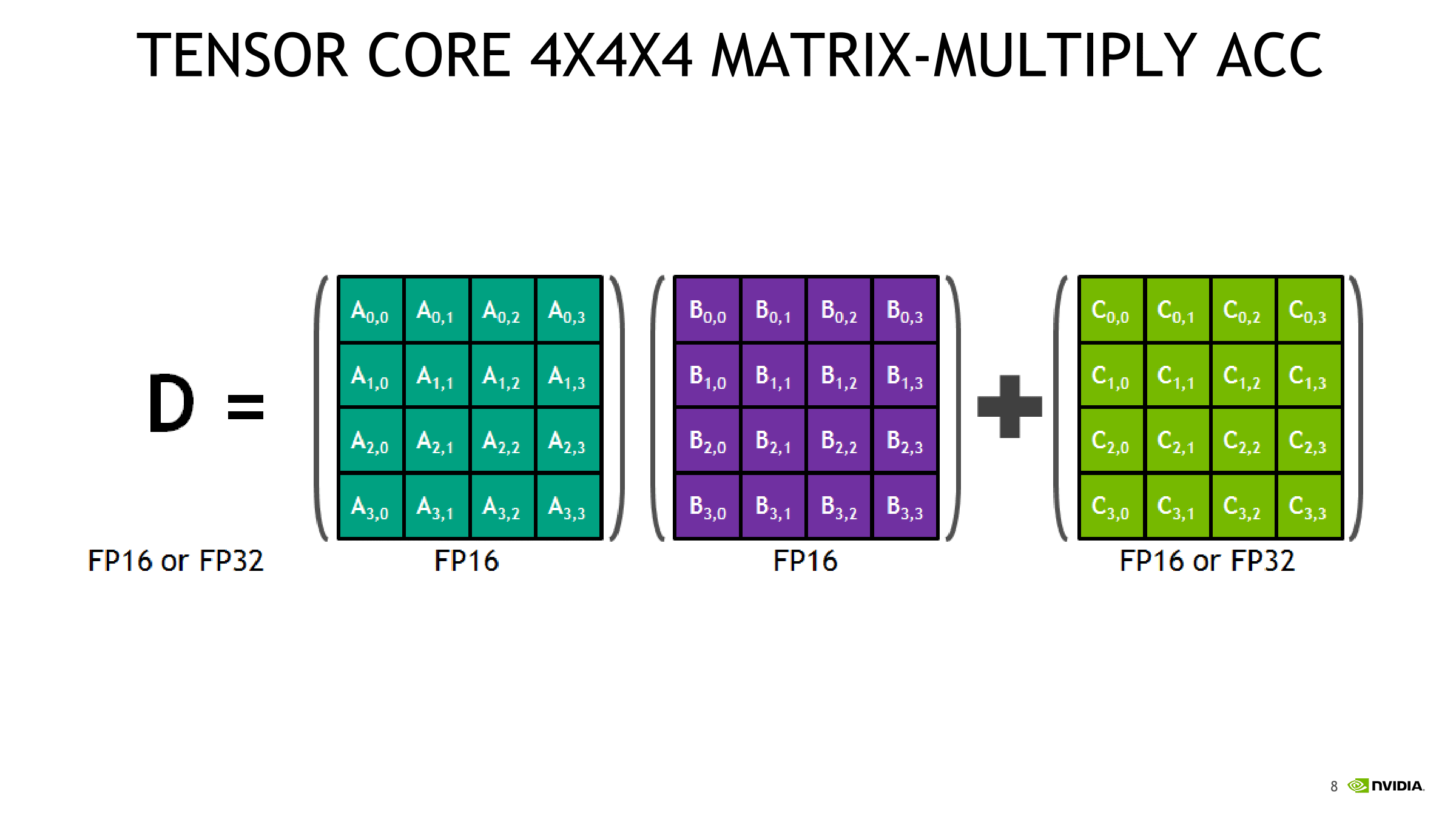
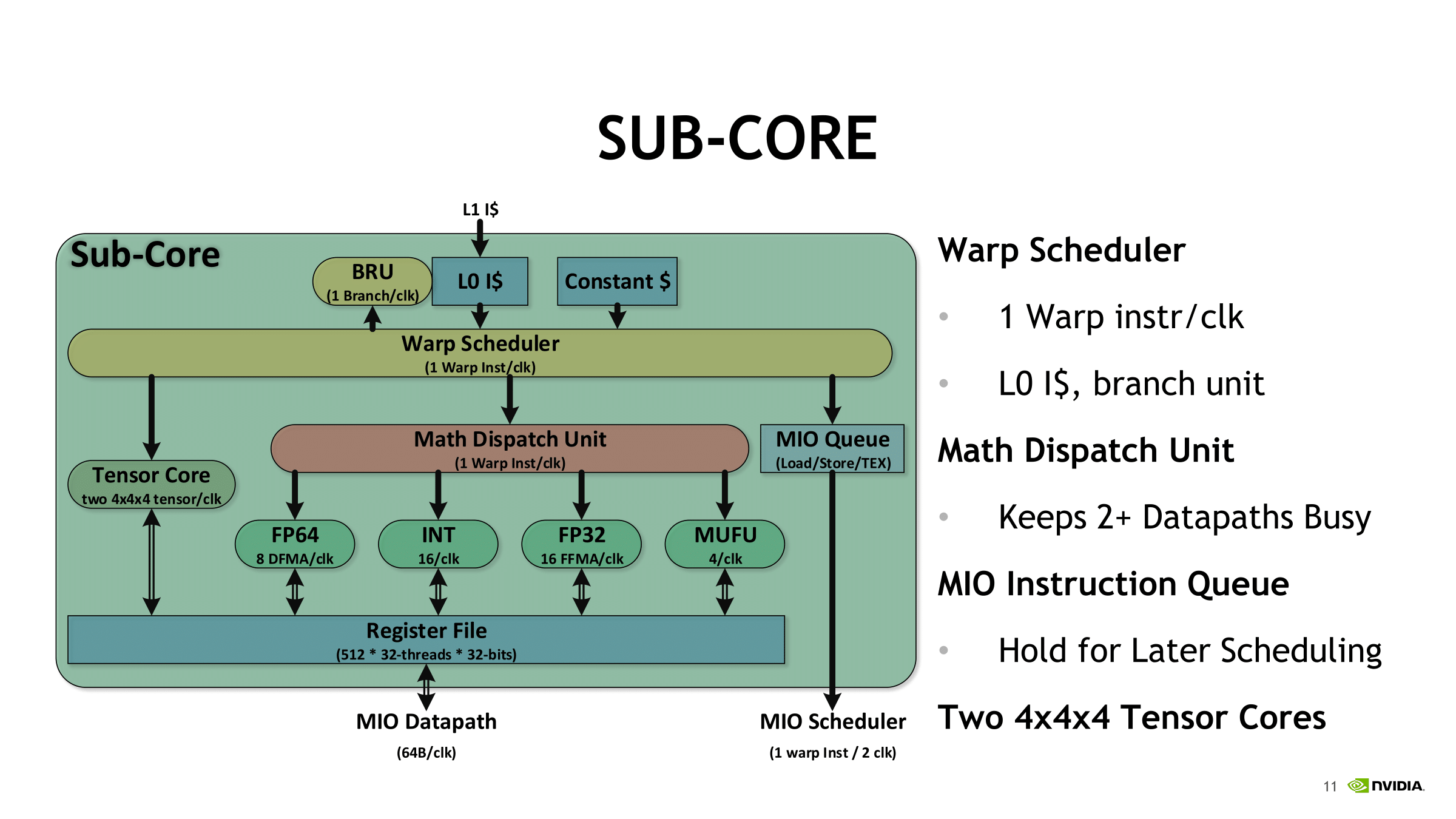
Consequently, while somewhat programmable, tensor cores are stuck to these types of 4 x 4 matrix multiplication-accumulation – and it’s not clear how and when the accumulation step occurs. Despite being described as doing 4 x 4 matrix math, in practice, tensor core operations always seem to be working with 16 x 16 matrices, with operations being handled across two tensor cores at a time. It appears that a lot of it has to do with the other changes in Volta, and more specifically, how these tensor cores are placed in an SM. For Volta, SMs were partitioned into four processing blocks, or sub-cores.
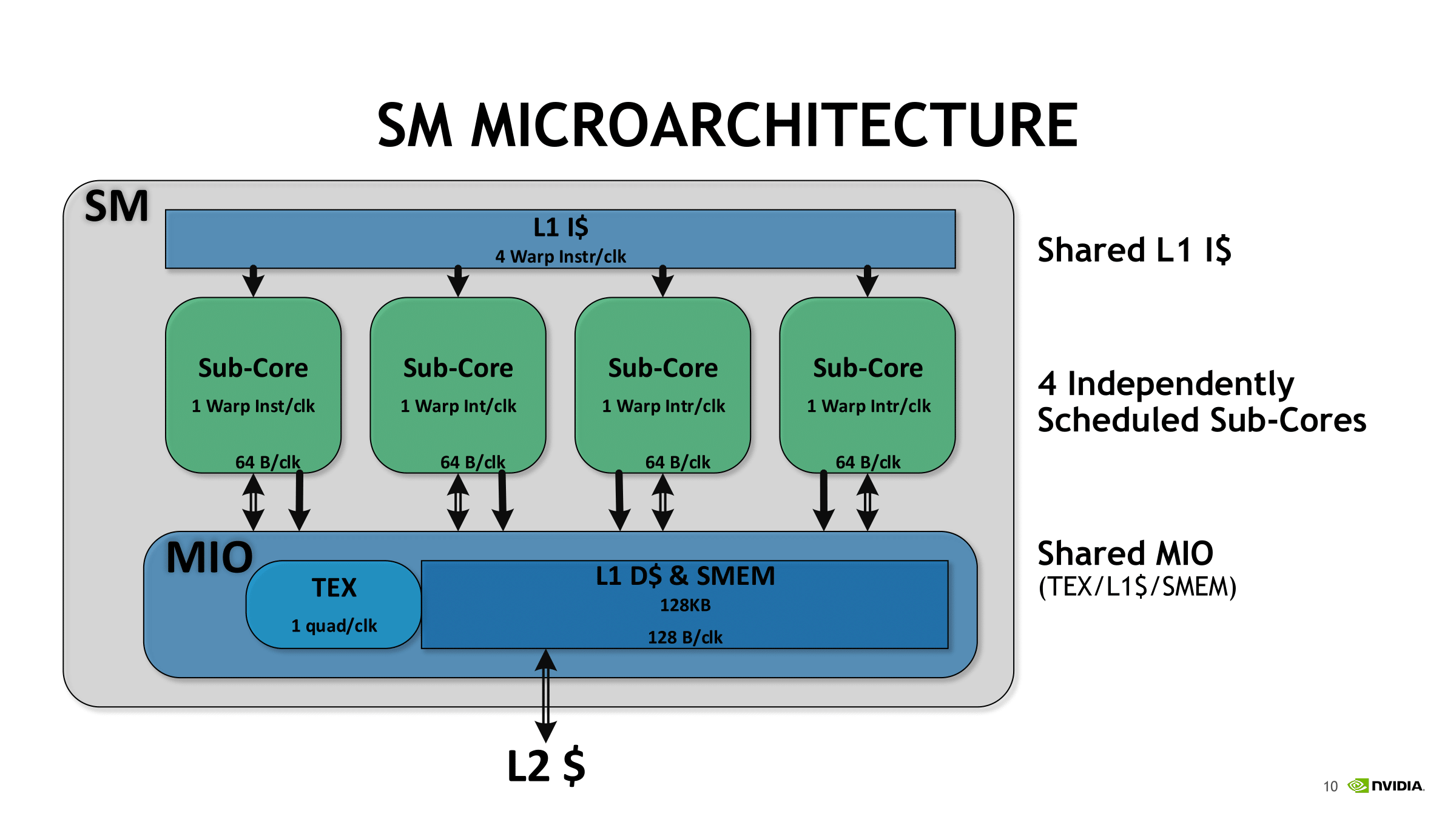
For each sub-core, the scheduler issues one warp instruction per clock to the local branch unit (BRU), the tensor core array, math dispatch unit, or shared MIO unit. For one, this precludes issuing a combination of tensor core operations and other math simultaneously. In utilizing the two tensor cores, the warp scheduler issues matrix multiply operations directly, and after receiving the input matrices from the register, perform 4 x 4 x 4 matrix multiplies. Once the full matrix multiply is completed, the tensor cores write the resulting matrix back into the register.
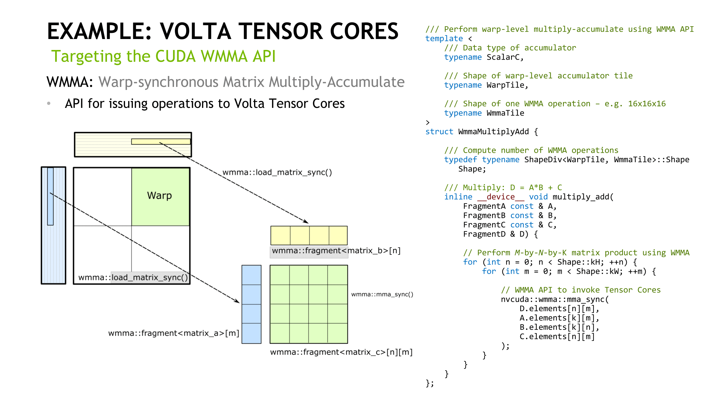
Looking at how tensor cores execute the actual instruction, opcode HMMA, only seems to raise more questions. Even at the compiler level with NVVM IR (LLVM), there are only intrinsics for warp-level matrix operations, rather than tensor cores, and warp-level remains the only level with CUDA C++ and the PTX ISA. Loading the input matrices is in the form of each warp thread holding a fragment, whose distribution and identity is unspecified. So broadly-speaking, it follows the same pattern of thread-level tiling-based GEMM computation for standard CUDA cores, and we'll circle back on that with NVIDIA's CUTLASS library in a moment.
In general terms, though, given the A*B+C tensor core operation, fragments consist of 8 FP16x2 elements (i.e. 16 FP16 elements) for A and another 8 FP16x2 elements for B, as well as 4 FP16x2 elements for an FP16 accumulator or 8 FP32 elements for an FP32 accumulator.

After the matrix multiply-accumulate operation, the result is spread out in fragments in the destination registers of each thread. Requiring warp-wide unity, these low-level operations essentially fail if one of the warp threads had exited.
Low-level microbenchmarking by a team at Citadel LLC revealed a number of Volta microarchitecture details, including tensor core operations and the fragments involved, both locations in the register and identity compared to the input matrices. They observed that a sub-core proceeds to calculate the matrix-multiply in a particular patchwork pattern, with all 32 threads of the warp in action. Conceptually, the tensor cores operate on 4 x 4 submatrices to calculate the larger 16 x 16 matrix, involving Volta’s cooperative groups and new scheduling model.
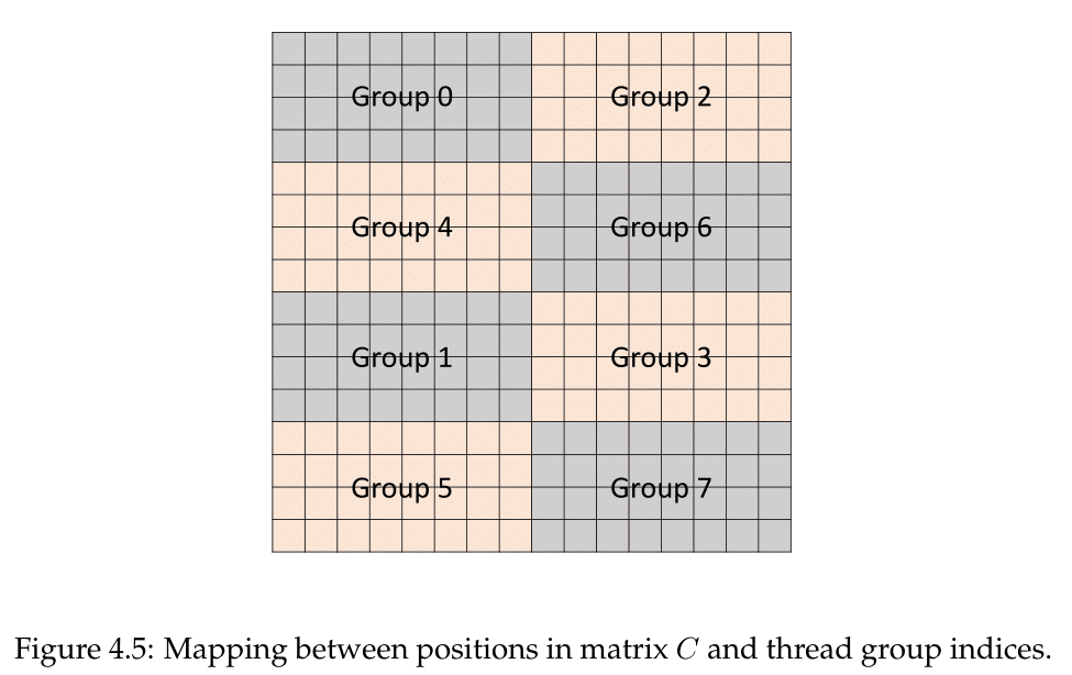
With the warp threads separated out into 8 thread groups of 4 threads, each thread group computed an 8x4 chunk serially, going through a process of 4 sets. So altogether, each thread group dealt with 1/8 of the resultant matrix.

Within a set were four HMMA steps that could be done in parallel, each applying to a 4x2 subchunk. The four threads were directly linked to those matrix values in the register, so that a single Step 0 HMMA instruction could be processed by the thread group to compute the subchunk in one go.

As matrix multiplication mathematically requires reuse of certain columns and rows, to permit parallel execution across all 8x4 chunk each 4 x 4 matrix is mapped to the registers of two threads. If applicable, the accumulate step sums the product with a stored accumulator; in this case of 4 x 4 submatrix operations to calculate a 16 x 16 parent matrix, this would include summing the sets as they were computed serially to form the corresponding chunk of 4 x 8 elements in the 16 x 16 matrix. Though untested by Citadel, it has been observed that FP16 HMMA instructions result in 2 steps rather than 4, relating to the smaller register space that FP16 occupies, and presumably a similar principle applies. Assuming that the sub-core was configured for peak output, it’s still hard to estimate without numbers, though it seems like ‘FMA ops per cycle’ is in reference to the matrices’ constituent values.
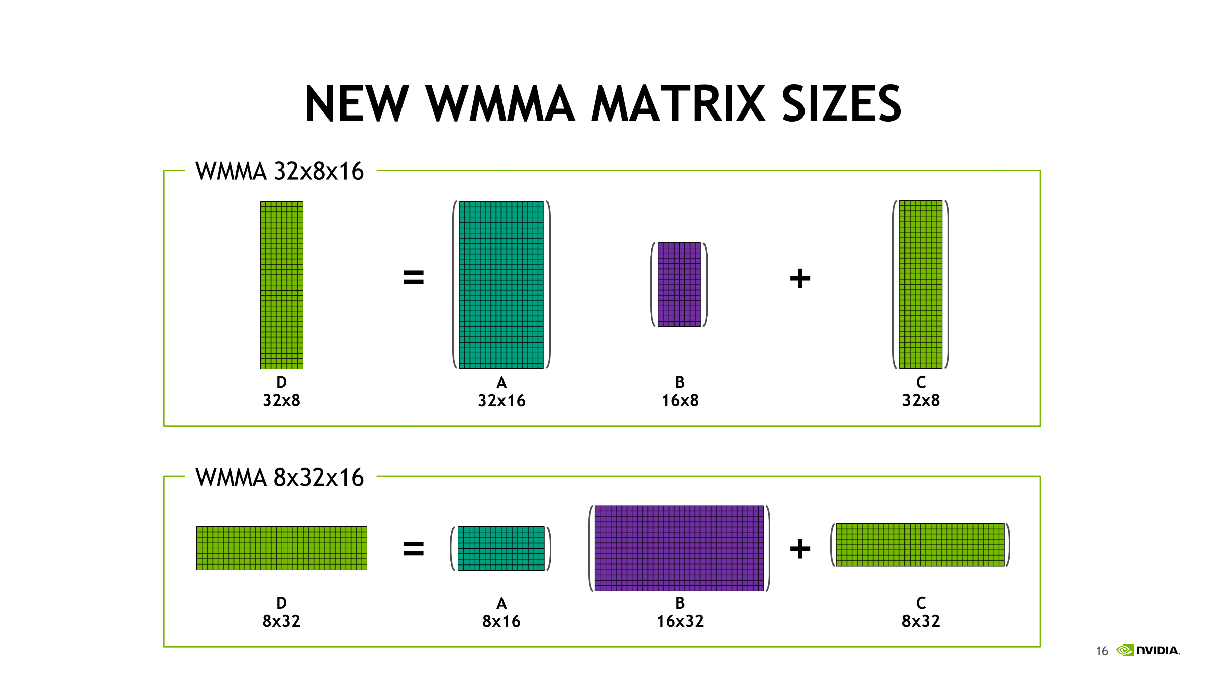
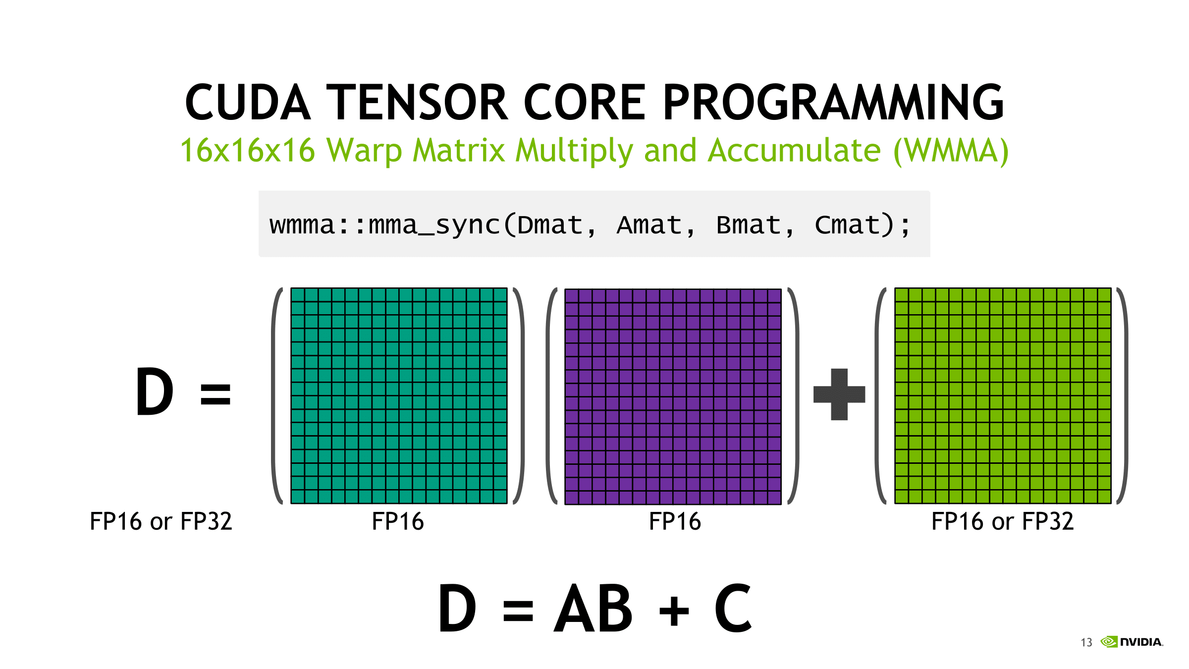
With independent thread scheduling and execution, as well as warp synchronization and warp-wide result distribution, the basic 4 x 4 x 4 tensor core operations translate into semi-programmable 16 x 16 x 16 mixed precision matrix multiply-accumulation, though with CUDA 9.1, 32 x 8 x 16 and 8 x 32 x 16 configurations are supported. For both new shapes, the multiplied matrices need the appropriate corresponding columns and rows of 16, with the end matrix being 32 x 8 or 8 x 32; this more-or-less suggests that standalone 4 x 4 x 4 matrix multiply-accumulate operations can’t be easily supported. Hard-coded warp-level behavior of register fragments, implementation of the MMA instruction, or tensor core ALUs could easily result in solely warp-level tensor core matrix math. And from a practical viewpoint, power consumption would suffer due to the increased register file usage while not significantly adding to deep learning performance.
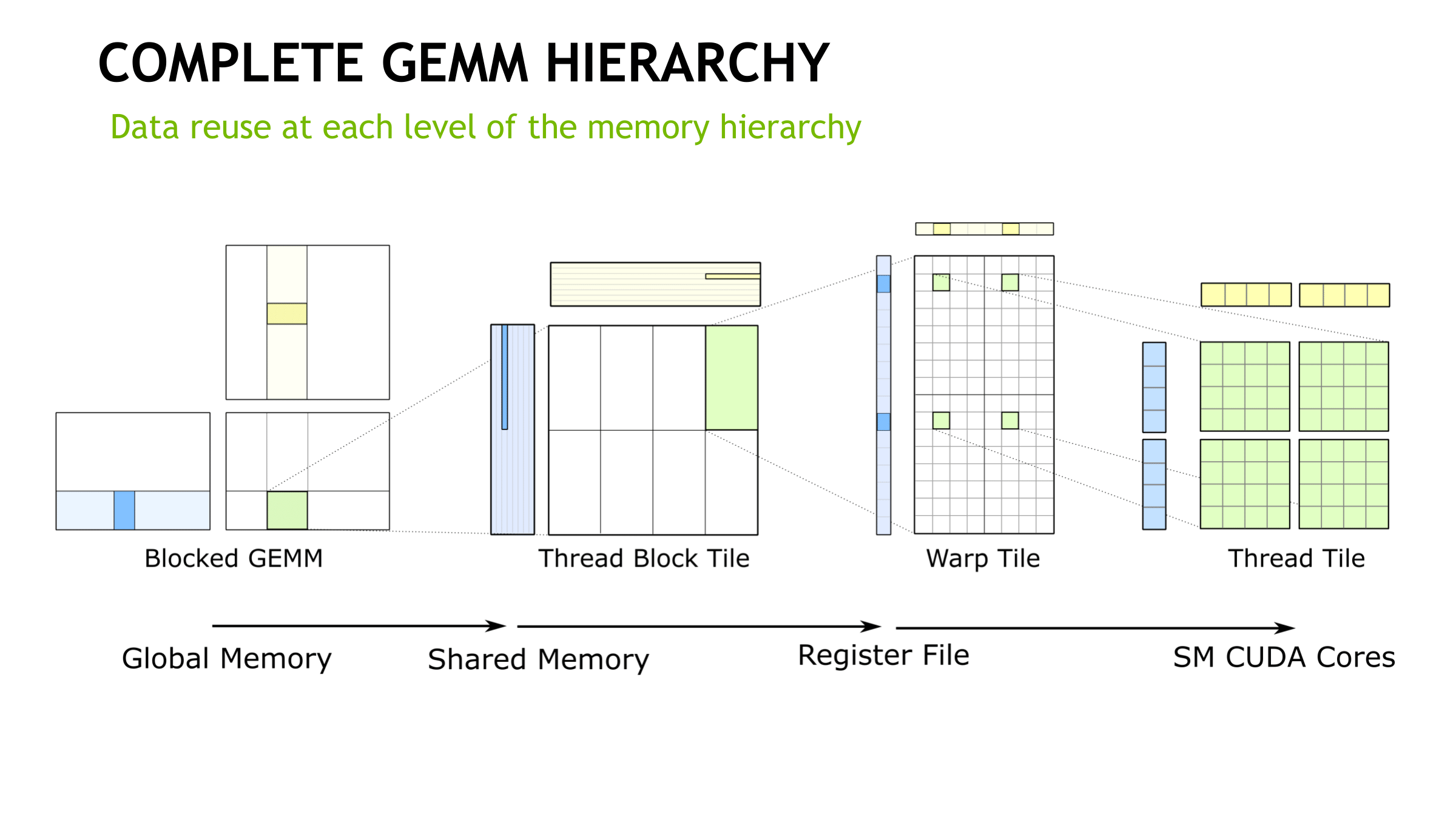
How tensor cores operate seem to be a hardware implemented step of NVIDIA's GEMM computation hierarchy, as seen in CUTLASS, their CUDA C++ template library for GEMM operations. With traditional CUDA cores, the last step requires breaking down (i.e. 'decomposing') the warp tile structure into scalar and vector elements owned by individual threads. With the WMMA API, which right now means tensor cores, all that is abstracted away, leaving only the warp-cooperative matrix fragment load/store and multiply-accumulate to deal with. The accumulation occurs in-place as an FMA-type operation.
On the register level, NVIDIA themselves mentioned in their Hot Chips 2017 paper that “with three relatively small 4x4 matrices of multiply and accumulator data, 64 multiply-add operations can be performed.” And the per-thread program counter of the enhanced Volta SIMT model, something that enables tensor cores, usually requires 2 register slots per thread according to the whitepaper. There also may have been a change to the register structure; a 2-bank 64-bit configuration was reported by Citadel, though NVIDIA themselves have documented 4-bank 32-bit. The HMMA instructions themselves feature as much register reuse as possible, despite the other Volta enhancements (that we’ll touch on in a moment), so I can’t imagine registers aren’t bottlenecking tensor cores for the majority of cases.
For standalone 4 x 4 matrix multiply-accumulate, I suspect that the tensor core array was not physically designed for it in terms of registers, data paths, and scheduling, such that it is only useable with specific submatrix multiplications (though admittedly I’ve not studied linear algebra in some time).
In any case, from NVIDIA’s point-of-view, Volta isn’t a deep learning ASIC; it is still covering the GPGPU space, and so keeping to CUDA programmable tensor cores for applicability to GEMM/cuBLAS and HPC is only logical. With CUTLASS for CUDA C++, this is even more the case, as its WMMA API support is aimed at enabling tensor core GEMM operations for a broad range of applications. Fundamentally, the development of NVIDIA's deep learning hardware acceleration has much to do with the development of cuDNN (and cuBLAS, to a lesser extent) over the years.
-01_thumb.png)
-02_thumb.png)
-03_thumb.png)
-04_thumb.png)
-05_thumb.png)
-06_thumb.png)


65 Comments
View All Comments
Nate Oh - Wednesday, July 11, 2018 - link
Thanks for your inquisitive responses throughout :)And yes, I was trying to be impartial with AMD's claims about deep learning. Until I have results myself, I offer them a degree of the benefit of the doubt, considering their traditional GPGPU capabilities. Meaning that "image classification for machine learning..." essentially falls under all the deep learning investigations I did for the review. My personal opinion is that 8-bit SAD will be as useful as it was with Kepler/Maxwell in terms of DL acceleration, except with lesser software support; you can make of that as you will. It really gets into the weeds to put AMD's 'machine intelligence' terminology under the scope, and I'd feel more comfortable doing so in an AMD-focused DL/ML investigation. I want to emphasize again that new instructions matter much less in the context of software/library/API support, so the fact that they are absent from the whitepaper directly adds to that observation. If this were a Vega FE DL review, I would certainly pester AMD about that, as much as I put an effort towards TensorRT and FP16 storage/tensor cores here. So encourage AMD to sample me :D
>TFLOPS
It is TFLOPS just for DeepBench because that is how Baidu and NV/AMD/Intel present their DeepBench results; you can see for yourselves at the DeepBench Github. We have not independently configured results (for DeepBench) that way, and I apologize if that's how it came across. This also makes it easier to keep us accountable by comparing our results to Baidu's Github. DeepBench is, as stated in the article, completely framework and model agnostic. We use TFLOPS when it is floating point, and we actually use TOPS when it is integer :) I've generalized a bit only because that comment had become so lengthy. This TFLOPS/TOPS usage is limited to solely DeepBench because of how they use pure math kernels, and precisely the reason I included end-to-end results with DAWNBench implementations.
>Open source
Indeed, like I've said, I've actually gone and attempted (poorly) to do some dev work myself. The article could *easily* ballooned to double the length, as well. The point I wanted to convey is exactly what you've picked up with AMD. Given the limited scope of the article (and the lack of direct AMD DL investigations), I want to refrain from saying something outright like, 'one of the main reasons we don't currently use AMD,' but I am just aware as you are on this point :) This deduction is unsaid but present throughout, .
Nate Oh - Wednesday, July 11, 2018 - link
Clarification: "so the fact that citations are absent from the whitepaper"mode_13h - Thursday, July 12, 2018 - link
> I was trying to be impartial with AMD's claims about deep learning. Until I have results myself, I offer them a degree of the benefit of the doubt, considering their traditional GPGPU capabilities.As a member of the tech press, please don't forget your privileged position of being able to request guidance on how to exercise claimed product features. I think this is a fair question and wouldn't impart any bias. Rather, it would help inform readers of how to exploit these features, and also quantify product performance when used as the designers intended.
I think it's also fair to ask if they can provide any references (either implementations or papers) to support their claims regarding how SAD can be utilized in machine learning, in cases of doubt.
Again, I'm saying this mostly in anticipation of your future Vega coverage, whether you choose to follow up with Vega 10, or perhaps you only revisit the matter with Vega 20.
As for searching & sifting through the sources of MIOpen, I think that's "over and above" what's expected. I'm just pointing out that, sometimes, it's actually surprisingly easy to answer questions by doing simple text searches on the source code. Sometimes, like when checking whether a certain instruction is emitted, it's also possible to save the generated assembly language and search *that*.
Demiurge - Friday, July 20, 2018 - link
Nate gets paid to educate and discuss with you, I don't, but more importantly to me, I made my point that Vega is not "underwhelming" for DL.Why should I *convince* you? I don't *need* to convince you. You didn't state Vega was "underwhelming" for DL.
Nate Oh - Monday, July 9, 2018 - link
To put it lightly, use of FP16 in DL training is not on the same level of use of INT8 in training; the latter is basically pure research and highly niche to those specific implementations. FP16 training (with NVIDIA GPUs) has reached a level of maturity and practicality where there is out-of-the-box support for most major frameworks. FP16 training and INT8 inferencing is the current understanding of lower-precision applicability in DL.More specifically, the whole field of lower-precision DL training/inference is all about making lower-precision datatypes more important, so of course that's the case for INT8/FP8. FP16 is already relevant for real-world training in certain scenarios; some researchers are *trying* to make INT8 relevant for real-world training in certain scenarios. As mode_13h said, that paper is a custom 8-bit datatype used to approximate 32-bit gradients for parameter updates during the backprop, specifically to speed-up inter-GPU communication for greater parallelism. AKA it is not usage of 8-bit datatypes all around, it's very specific to one aspect. It's essentially a proof-of-concept and pure research. Using INT16 for everything is hard enough; some people (see below) were able to use a custom INT16 format and use INT16/INT32 FMA. And yes, sometimes, companies don't distinguish inference and training as clearly as they should, with the resulting perception of superior general DL performance.
In any case, DP4A is not really used in training at all and it wasn't designed to do so anyway. You can ‘make’ the exception with research papers like what you cited but you can always find niche exceptions in research because that is its purpose. It was designed for inferencing acceleration and as product segmentation for non-GP100 GPUs. Even now, it's pushed for working with a model that TensorRT converted from higher-precision to INT8.
(I am splitting this comment up to respond separately on the topic of Vega/instruction set support, but both comments should be considered in tandem)
References/Links
https://software.intel.com/en-us/articles/lower-nu...
https://ai.intel.com/lowering-numerical-precision-...
http://dawn.cs.stanford.edu/2018/03/09/low-precisi...
https://www.tensorflow.org/performance/quantizatio...
https://arxiv.org/pdf/1802.00930.pdf (Custom datatype for INT16/INT32 mixed precision training)
http://on-demand.gputechconf.com/gtc/2017/presenta...
https://devblogs.nvidia.com/int8-inference-autonom...
https://devblogs.nvidia.com/mixed-precision-progra... (Introduction of DP4A/DP2A)
mode_13h - Tuesday, July 10, 2018 - link
> ... DP4A is not really used in training at all ... It was designed for inferencing acceleration and as product segmentation for non-GP100 GPUs.You mean segmentation of GP100 vs. GP102+ ? Or are you saying it's lacking in some of the smaller Pascal GPUs, like GP107? And *why* isn't it listed in the CUDA compute capabilities table (https://docs.nvidia.com/cuda/cuda-c-programming-gu... Grrr!
Regardless, given that GV100 has it, I get the sense that it was simply an evolution that came too late for the GP100.
Finally, thank you for another thoughtful and detailed reply.
Ryan Smith - Tuesday, July 3, 2018 - link
The Titan V is such a niche card that I'm not surprised to hear NV hasn't prepared macOS drivers. There are good reasons for them to have drivers ready for their consumer hardware - they need to do the work anyhow to support existing products and make sure they're ready to take a new Apple contract if they win it - but the Titan V/GV100 will never end up in a Mac. So adding that to the mac drivers would be a less beneficial decision.Flunk - Tuesday, July 3, 2018 - link
I'm surprised any cards not shipped in Mac Models have Mac drivers anymore. It's not like you can add a PCI-E video card to any recent Mac.Strunf - Wednesday, July 4, 2018 - link
Thunderbolt allows for an external PCI-E card but there's probably just a few guys ready to do this kind of thing...ImSpartacus - Tuesday, July 3, 2018 - link
Is the new 32GB V100 still on SXM2?Several sites mentioned SXM3 in reference to the 32GB refresh of V100, but it's hard to find details on what improved (if anything).