Cambricon, Makers of Huawei's Kirin NPU IP, Build A Big AI Chip and PCIe Card
by Ian Cutress on May 26, 2018 5:00 PM EST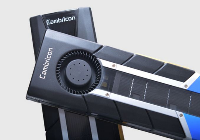
Cambricon Technologies, the company in collaboration with HiSilicon / Huawei for licensing specialist AI silicon intellectual property for the Kirin 970 smartphone chipset, have gone solo and created their own series of chips for the data center.
The IP inside the Kirin 970 is known as Cambricon-1A, the company’s first licensable IP. At the time, finding information on Cambricon was difficult: its website was a series of static images with Chinese embedded into the image itself. Funnily enough, we used the AI-accelerated translate feature on the Huawei Mate 10 to translate what the website said. Fast forward 12-18 months, and the Cambricon website is now interactive and has information about upcoming products. A few of which were announced recently.
The Big Chip: Going for Data Center
Built on TSMC’s 16FF, the MLU-100 is an 80W chip with a capability of 64 TFLOPS of traditional half-precision or 128 TOPS using the 8-bit integer metric commonly used in machine learning algorithms. This is at 1.0 GHz, or the ‘standard’ mode – Cambricon’s CEO, Dr Chan Tianshi, stated that their new chip has a high-performance mode at 1.30 GHz, which allows for 83.2 TFLOPS (16-bit float) or 166.4 TOPS (8-bit int) but rises to 110W. This technically decreases performance efficiency, but allows for a faster chip. All this data relies on sparse data modes being enabled.
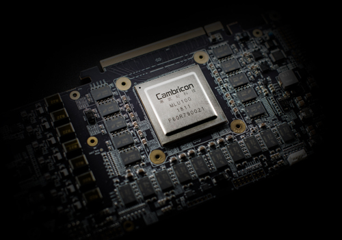
The technology behind the chip is Cambricon’s latest MLUv01 architecture, which is understood to be a variant of the Cambricon-1A used in the Kirin chipsets but scaled to something bigger and faster. Obviously additional rules have to be implemented for data and power management compared to the mobile IP. Cambrian also has its 1H architecture and newly announced 1M architecture, although there is no disclosure as to how these might relay to the chip.
David Schor from WikiChip (the main source of this article) states that this could be NVIDIA’s first major ASIC competition for machine learning, if made available to commercial partners. To that end, Cambricon is also manufacturing a PCIe card.
| Specification Comparison | ||||||
| AnandTech | Cambricon MLU100-Base |
Cambricon MLU100-Perf |
Tesla V100 (SXM2) |
Tesla V100 (PCIe) |
||
| CUDA Cores | - | 5120 | 5120 | |||
| Tensor Cores | - | 640 | 640 | |||
| Core Clock | 1.0 GHz | 1.3 GHz | ? | ? | ||
| Boost Clock | - | 1455MHz | 1370MHz | |||
| Memory Clock | DDR4-1600 | 1.75Gbps HBM2 | 1.75Gbps HBM2 | |||
| Memory Bus Width | 256-bit | 4096-bit | 4096-bit | |||
| Memory Bandwidth | 102.4GB/sec | 900GB/sec | 900GB/sec | |||
| VRAM | 16GB 32GB |
16GB 32GB |
16GB 32GB |
|||
| L2 Cache | - | 6MB | 6MB | |||
| Half Precision | 64.0 TFLOPS | 83.2 TFLOPS | 30 TFLOPS | 28 TFLOPS | ||
| Single Precision | - | 15 TFLOPS | 14 TFLOPS | |||
| Double Precision | - | 7.5 TFLOPS | 7 TFLOPS | |||
| Deep Learning | 128.0 TOPS | 166.4 TOPS | 120 TFLOPS | 112 TFLOPS | ||
| GPU | - | GV100 | GV100 | |||
| Transistor Count | ? | 21B | 21B | |||
| TDP | 80 W | 110 W | 300W | 250W | ||
| Form Factor | PCIe | SXM2 | PCIe | |||
| Cooling | Active | Passive | Passive | |||
| Process | TSMC 16FF | TSMC 12FFN | TSMC 12FFN | |||
| Architecture | Cambricon-1? | Volta | Volta | |||
Obviously NVIDIA has a strong user base and multiple generations at this, along with the software in hand to take advantage of their hardware. Cambricon did not go into detail about how they plan to support any SDKs for the new chip, however it does have a series of SDKs on its website, supporting TensorFlow, Caffe, and MXNet.
Getting Into the Data Center: PCIe
The best way to be plug and play in a data center is through a PCIe card. Cambricon’s MLU100 accelerator card is just that: a PCIe 3.0 x16 enabled implementation with either 16 or 32 GB of DDR4-3200 memory on a 256-bit bus, which is good for 102.4 GB/s of bandwidth. To get that much memory on NVIDIA requires the high end cards, but those cards offer multiple times the memory bandwidth. The memory on the MLU100 card has ECC enabled also.

The reports so far state that Lenovo is offering the cards as add-ons to its ThinkSystem SR650 dual Intel Xeon servers; up to two per machine. Looking on the Lenovo website it does not look like they are available quite yet. Given Huawei’s big enterprise presence, it is likely that we might see the chips in those systems as well.
Next Generation: 5 TOPS/Watt
Also reported was the new Cambricon-1M product IP, although the company was not forthcoming with details. WikiChip states that this new IP is built primarily for 7nm, so we are likely to see it when Huawei/HiSilicon starts shipping 7nm mobile processors and then into the next generation of server-focused products. The goal for this IP is to hit 5 TOPS/Watt, compared to the 3 TOPS/Watt advertised by ARM's IP. David also states that Cambricon has a training and inference chip planned for later this year, with another update in 2019.
Related Reading
- HiSilicon Kirin 970 - Android SoC Power & Performance Overview
- Hands-on & More With Huawei's Mate 10 and Mate 10 Pro: Kirin 970 Meets Artificial Intelligence
Source: WikiChip, Cambricon 1, Cambricon 2


25 Comments
View All Comments
Dragonstongue - Saturday, May 26, 2018 - link
thats insane, but just goes to show what is capable with a focused design instead of trying to pick and choose what it will support or not support in your face ngreedia....that being said, I can only imagine what kind of insane design AMD could come up with when/if it says "f it, make an all out compute specific graphics accelerator" because as it stands they are guilty as well of trying to "do it all".with AMD I can "kind of" understand because they have many frying pans in many fires, Nv has nowhere near that same excuse because they have ALWAYS (to my knowledge) been focused on graphics and graphics alone (very short amount of time with motherboard chipsets which they very much did as little as possible and overpriced for what was given (load of issues, overheating etc)
anyways.....that is some serious horsepower on these considering very low amount of memory bandwidth and TDP...I so wish they would get rid of that stupid designation because they can easily blow past this amount or be under it 9/10....they need a "watt limited" number or something like that instead ^.^
mode_13h - Tuesday, May 29, 2018 - link
You might be reading too much into the headline numbers. There are a couple of key phrases, like:"All this data relies on sparse data modes being enabled."
Which tells me their headline numbers might not be sustainable, in the general case, and perhaps you need exactly the right network architecture to get close to the theoretical compute numbers.
It does make one wonder whether Nvidia will try excluding things like fp64 and geometry engines, to make a truly purpose-build deep learning chip.
bryanlyon - Saturday, May 26, 2018 - link
I think it's important to note that the Volta line (including the V100) actually have a specialized Ai Tensor Cores that actually mean the AI speed is approximately 120 TFLOPS not the 30 TFLOPS for generic CUDA.ToTTenTranz - Sunday, May 27, 2018 - link
Regarding the chart, I wouldn't say Cambricon's solution uses "VRAM".Valantar - Sunday, May 27, 2018 - link
Came here to say the same thing. VRAM = Video RAM, right? There's nothing video related here (even if the chip were used for facial recognition or other video-based work), so calling it "compute RAM" or something like that would seem more fitting, no?Yojimbo - Sunday, May 27, 2018 - link
Not the firs time a term became bastardized and it won't be the last. It's not being used for video anything in the V100, either, under the contexts in which the comparisons are being made.The important thing is that it is on-board RAM and not system RAM.
bananaforscale - Sunday, May 27, 2018 - link
"Memory clock"... Yeah, 1600 is strictly correct (DDR4 isn't, that's a technology), what it means tho is DDR4-3200 memory. That table could've been so much better if a bit more thought had gone into naming the rows.wr3zzz - Monday, May 28, 2018 - link
How big a hurdle is it from making something like this to GPU?vladx - Monday, May 28, 2018 - link
Too high to be worth entering a very competitive market like GPU market as a new player today.mode_13h - Tuesday, May 29, 2018 - link
Have you heard of a company called Vivante?