ASML to Ship 30 EUV Scanners in 2019: Faster EUV Tools Coming
by Anton Shilov on January 28, 2019 3:00 PM EST- Posted in
- Semiconductors
- Intel
- SK Hynix
- EUV
- EUVL
- ASML
- TSMC
- 7nm
- Samsung Foundry
- 5nm
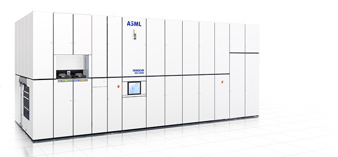
ASML said last week that it planned to ship 30 extreme ultraviolet scanners in 2019, up significantly from 2018. The plan is not surprising, as demand for EUV lithography tools is rising and semiconductors manufacturers are building new fabs. In addition, ASML indicated plans to introduce a new EUV scanner that will offer a higher production throughput, the NXE: 3400C.
Last year ASML shipped (only) 18 Twinscan NXE: 3400B EUV scanners. This was slightly below its expectations, to supply 20 machines. In total, as of July 2018, there were 31 EUV scanners installed at various fabs across the world, including several machines in various semiconductor research organizations, including imec. If everything goes as planned, ASML will ship more extreme ultraviolet scanners in 2019 than it did in in years before that.
Samsung Foundry has already started to use ASML’s EUV equipment for production of commercial chips using its 7LPP process technology at its Fab S3. As reported, a major increase of EUV lithography use by Samsung will commence after it builds another production line in Hwaseong, which was architected for the EUV tools from the start. The fab is set to cost 6 trillion Korean Won ($4.615 billion), it is expected to be completed later this year, and start high volume manufacturing in 2020.
TSMC is set to start using its Twinscan NXE scanners for commercial wafers in the second half of this year to produce chips using its N7+ manufacturing technology. Initially EUV scanners will be used for non-critical layers, but their use will be expanded at the 5 nm node in 2020 – 2021. TSMC says that virtually all customers that use its N7 fabrication process will also use its N5 technology for their next-gen chips.
Demand for ASML’s Twinscan NXE tools will be further boosted by demand from Intel and SK Hynix. Intel will need EUV tools as it expands its fabs in Oregon, Israel, and Ireland. Besides, the chipmaker will need EUV scanners to equip its Fab 42 in Arizona. These factories will be used to produce chips using Intel’s 7 nm fabrication process. SK Hynix will need EUV tools for its new fab near Icheon, South Korea.
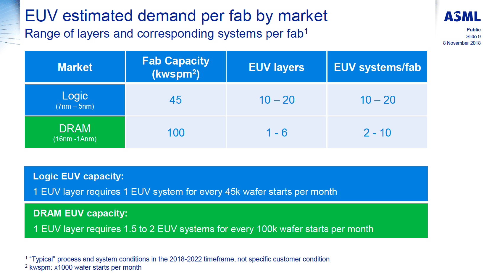
According to ASML, one EUV layer requires one EUV step-and-scan system for every ~45,000 wafer starts per month. As leading makers of semiconductors expand the use of EUV tools going forward, they will need additional scanners, which will naturally increase demand for ASML’s Twinscan NXE products.
Later this year ASML will introduce its new generation Twinscan NXE: 3400C EUV scanner that will be able to process 170 wafers per hour, up from 155 wafers per hour on the NXE: 3400B. The new scanner will use Cymer’s new 340 W light source, which will enable higher performance. ASML’s Twinscan NXE: 3400C will allow chip manufacturers to keep cycle times for their next-gen chips in check.
“We shipped six systems in Q4, which translates to a total of 18 EUV shipments in 2018,” said Peter Wennink, CEO of ASML, during a conference call last week. “With the five orders booked this quarter, our shipment plan of 30 systems for 2019 is covered. In DUV, we shipped 189 new systems in 2018, an increase of 17% over 2017 and we were able to further increase our output in support of the demand from both logic and memory customers. And we continued ramping our latest immersion system, NXT:2000 with a record time to achieve mature customer yields.”
Related Reading
- Intel: EUV-Enabled 7nm Process Tech is on Track
- Intel to Equip Fab 42 for 7 nm
- Samsung Starts Mass Production of Chips Using Its 7nm EUV Process Tech
- TSMC: First 7nm EUV Chips Taped Out, 5nm Risk Production in Q2 2019
- TSMC Starts to Build Fab 18: 5 nm, Volume Production in Early 2020
- ASML Ships Twinscan NXT:2000i Scanner for 7nm and 5nm DUV
- EUV Lithography Makes Good Progress, Still Not Ready for Prime Time
Source: ASML, Seeking Alpha


17 Comments
View All Comments
surt - Tuesday, January 29, 2019 - link
Because Intel has the knowledge, capability, and capitalization to use such a tool, and they don't.Eliadbu - Tuesday, January 29, 2019 - link
Even if they have the knowledge to make every Machine in the fab (which they do not ) there is way more than just having the machines and running them. Those are the leading manufacturing fabs not some clothes factory. There is so much to how design and develop the technology than just running the machine especially in those small nodes. In the past there were several manufacturers that produced chip in the leading nodes now we are left with just 3. Mostly because it is very complicated and very expensive to compete in these new nodes.iwod - Tuesday, January 29, 2019 - link
30 is Inline with expectation. After years of delay we are finally reaching EUV in production. Although 30 isn't a lot, Samsung and TSBC would have taken it all. Which is why I do not believe Intel will have 7nm EUV by 2020.Santoval - Tuesday, January 29, 2019 - link
2020? No, no way, that's way too early. Assuming they are going to release three generations of "fixed 10nm" (since the original 10nm node they employed for Cannon Lake is broken), one each for Sunny, Willow and Golden Cove, and also assuming that these three CPU generations are released in 2019, 2020 and 2021 respectively, with *no* delays for either, then 7nm should debut in 2022 with Ocean Cove.That's the "brand new" CPU design Jim Keller was hired to design. Now, if Golden Cove is a new architecture rather than a (twice) optimized Sunny Cove then they might release an optimized version of Golden Cove at 7nm in 2022 and then release Ocean Cove in 2023. It's also possible that Golden Cove is (or will be) the new name of Ocean Cove.
On the other hand, they might even release Golden Cove at 7nm, in order to narrow their widening "Moore's Lag gap", though I strongly doubt that. My prediction for release of Intel's 7nm node (I mean in high volume, not a "pull the wool over the eyes of investors release", like they did with Core i3-8121U) would be 2022 at the earliest and 2023 at the latest - assuming smooth 7nm sails.
iwod - Tuesday, January 29, 2019 - link
The 2020 was reference to how Intel keep stating 7nm is on schedule, and said they will jump on 7nm when it is ready. The previous Anandtech Interview already states their CPU design will no longer be node dependent.And just to point out TSMC's 5nm is scheduled for 2020 iPhone, and early 2021 for High Power node.
gizmo23 - Tuesday, January 29, 2019 - link
Welcome news. There's been a lot of work put into this. It's not just a matter of working out how to focus EUV but also how to to make it work in a production environment. Processing 30 or 40 wafers an hour isn't good enough for the fab guys. Wonder what ASML are going to do next?PeachNCream - Tuesday, January 29, 2019 - link
The company plans to make and sell more scanners next.