Imagination Announces A-Series GPU Architecture: "Most Important Launch in 15 Years"
by Andrei Frumusanu on December 2, 2019 8:00 PM ESTNew ISA & ALUs: An Extremely Wide Architecture
As mentioned, the ALU architecture as well as ISA of the new A-Series is fundamentally different to past Imagination GPUs, and in fact is very different from any other publicly disclosed design.
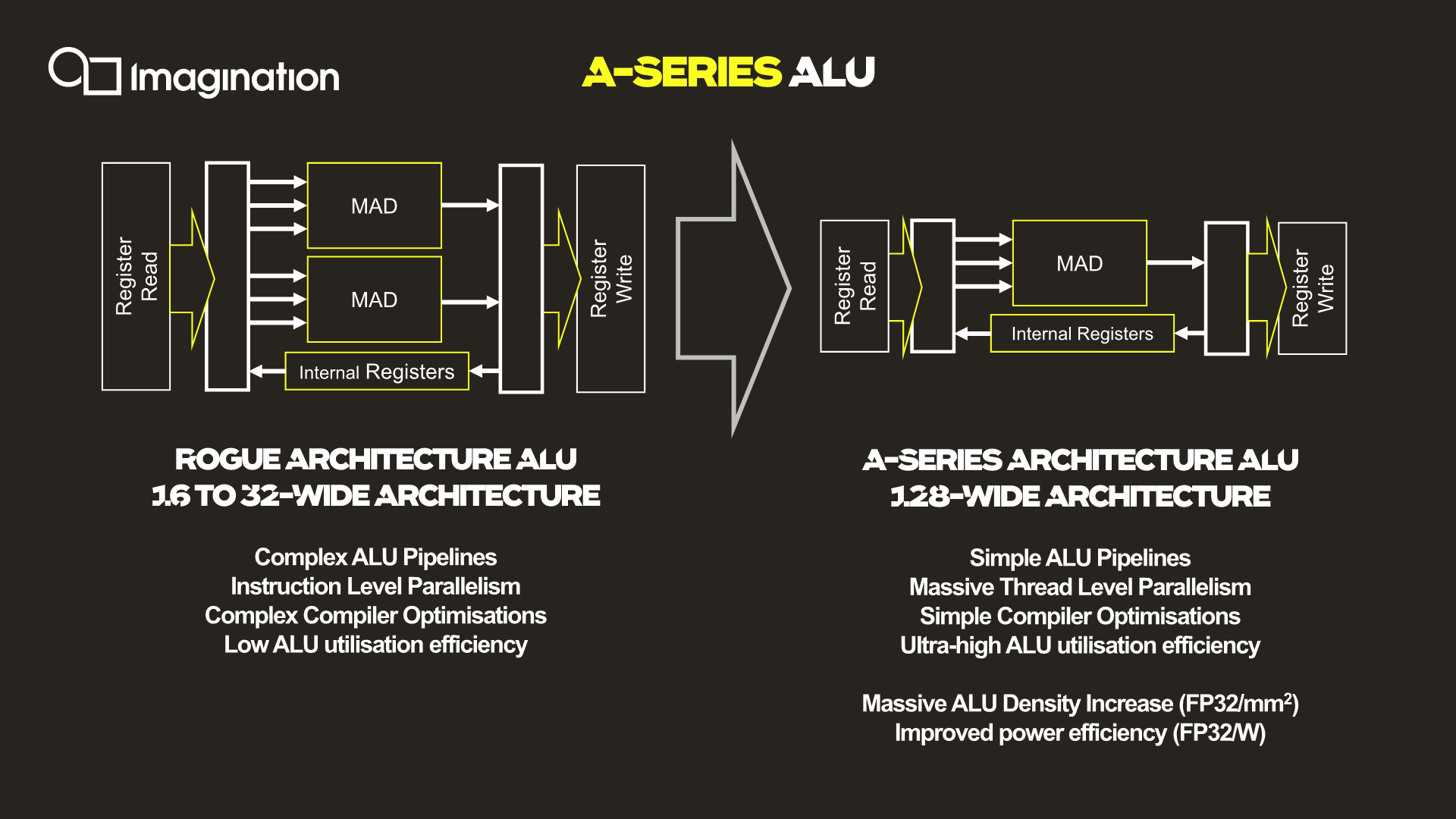
The key characteristic of the new ALU design is the fact that it’s now significantly wider than what was employed on the Rogue and Furian architectures, going to up a width of 128 execution units per cluster.
For context, the Rogue architecture used 32 thread wide wavefronts, but a single SIMD was only 16 slots wide. As a result, Rogue required two cycles to completely execute a 32-wide wavefront. This was physically widened to 32-wide SIMDs in the 8XT Furian series, executing a 32-wide wavefront in a single cycle, and was again increased to 40-wide SIMDs in the 9XTP series.
In terms of competing architectures, NVIDIA’s desktop GPUs have been 32-wide for several generations now, while AMD more recently moved from a 4x16 ALU configuration with a 64-wide wavefront to native 32-wide SIMDs and waves (with the backwards compatibility option to cluster together two ALU clusters/CUs for a 64-wide wavefront).
More relevant to Imagination’s mobile market, Arm’s recent GPU releases also have increased the width of their SIMDs, with the data paths increasing from 4 units in the G72, to 2x4 units in the G76 (8-wide wave / warp), to finally a bigger more contemporary 16-wide design with matching wavefront in the upcoming Mali-G77.
So immediately one might see Imagination’s new A-Series GPU significantly standing out from the crowd in terms of its core ALU architecture, having the widest SIMD design that we know of.
All of that said, we're a bit surprised to see Imagination use such a wide design. The problem with very wide SIMD designs is that you have to bundle together a very large number of threads in order to keep all of the hardware's execution units busy. To solve this conundrum, a key design change of the A-Series is the vast simplification of the ISA and the ALUs themselves.
Compared to the Rogue architecture as depicted in the slides, the new A-Series simplifies a execution unit from two Multiply-Add (MADD) units to only a single MADD unit. This change was actually effected in the Series-8 and Series-9 Furian architectures, however those designs still kept a secondary MUL unit alongside the MADD, which the A-Series now also does without.
The slide’s depiction of three arrows going into the MADD unit represents the three register sources for an operation, two for the multiply, and one for the addition. This is a change and an additional multiply register source compared to the Furian architecture’s MADD unit ISA.
In essence, Imagination has doubled-down on the transition from an Instruction Level Parallelism (ILP) oriented design to maximizing Thread Level Parallelism(TLP). In this respect it's quite similar to what AMD did with their GCN architecture early this decade, where they went from an ILP-heavy design to an architecture almost entirely bound by TLP.
The shift to “massive” TLP along with the much higher ALU utilization due to the simplified instructions is said to have enormously improved the density of the individual ALUs, with “massive” increases in performance/mm². Naturally, reduced area as well as elimination of redundant transistors also brings with itself an increase in power efficiency.
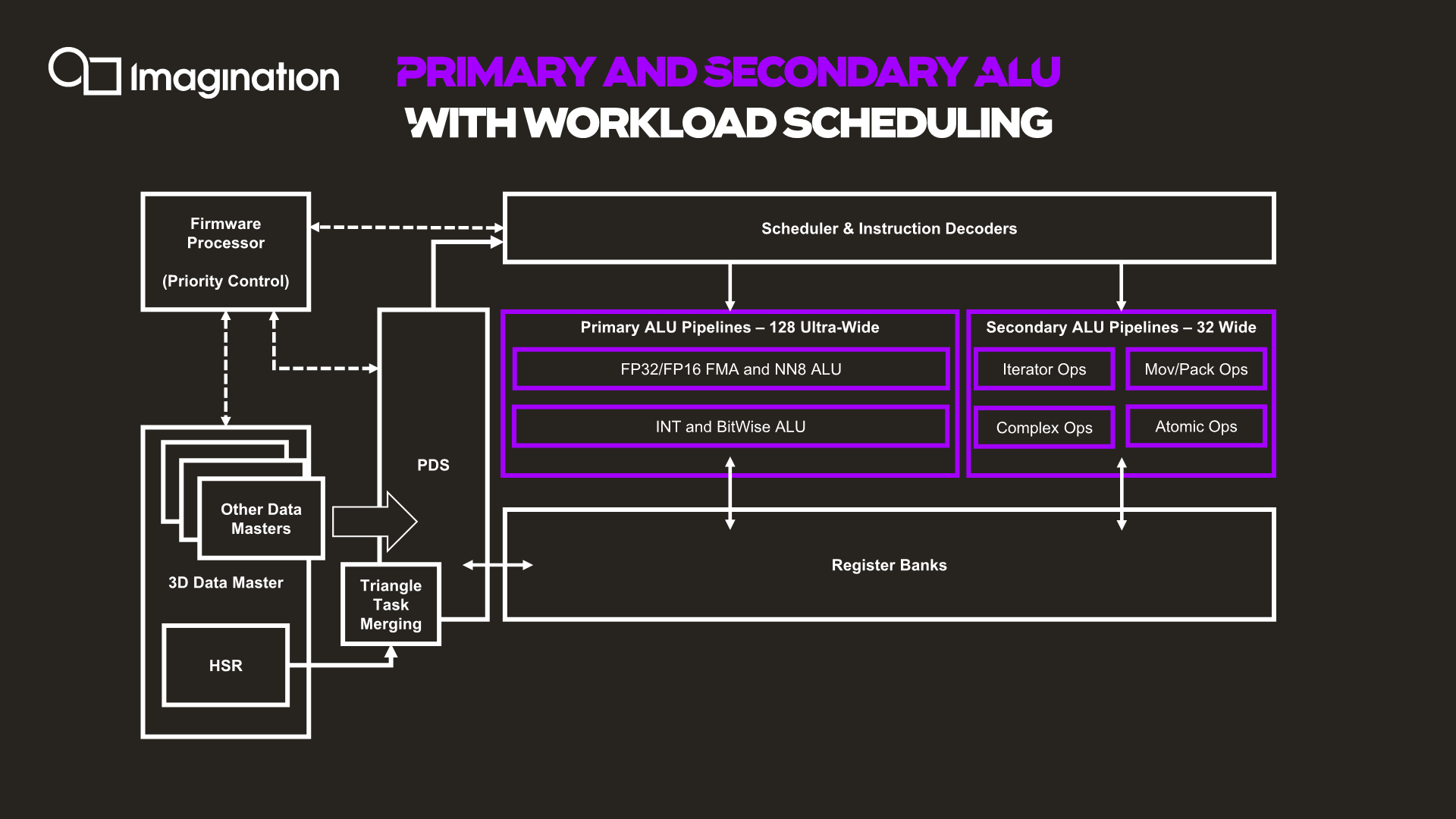
The next graphic describes the data and execution flow in the shader processor.
Things start off with a data master which kicks off work based on command queues in the memory. The 3D data master here also handles other fixed-function pre-processing, which will trigger execution of per-tile hidden surface removal and workload generation for the shader programs. The GPU here has a notion of triangle merging which groups them together into tasks in order to get better utilization of the ALUs and able to fill the 128 slots of the wavefront.
The PDS (Programmable Data Sequencer) is an allocator for resources and manager. It reserves register space for workloads and manages tasks as they’re being allocated to thread slots. The PDS is able to prefetch/preload data to local memory for upcoming threads, upon availability of the data of a thread, this becomes an active slot and is dispatched and decoded to the execution units by the instruction scheduler and decoder.
Besides the primary ALU pipeline we described earlier, there’s a secondary ALU as well. First off, a clarification on the primary ALUs is that we also find a separate execution unit for integer and bitwise operations. These units, while separate in their execution, do share the same data paths with the floating-point units, so it’s only ever possible to use one or the other. These integer units are what enable the A-Series to have high AI compute capabilities, having quad-rate INT8 throughput. In a sense, this is very similar to Arm’s NN abilities on the G76 and G77 for integer dot-product instructions, although Imagination doesn’t go into much detail on what exactly is possible.
The secondary pipeline runs at quarter rate speed, thus executing 32 threads per cycle in parallel. Here we find the more complex instructions which are more optimally executed on dedicated units, such as transcendentals, varying operations and iterators, data conversions, data moving ops as well as atomic operations.


143 Comments
View All Comments
Korguz - Tuesday, December 3, 2019 - link
and your not ?? come one melgross.. some of your posts... have pro intel all over them...Korguz - Tuesday, December 3, 2019 - link
case on point : https://www.anandtech.com/show/15162/dell-intel-cp...s.yu - Tuesday, December 3, 2019 - link
Ok? Like how HiSilicon siphoned from Cambricon?levizx - Tuesday, December 3, 2019 - link
How? It's a completely different architecture.vladx - Wednesday, December 4, 2019 - link
Don't mind s.yu, he's the biggest Chinese hater on AnandTech. You would save yourself time and energy just ignoring his rambling.s.yu - Wednesday, December 4, 2019 - link
Yeah...I vaguely remember you vlad, you were singing praises for the Soviet Union and claiming that China is the best everywhere and that its government takes care of every aspect of your life from housing to employment."Chinese hater"
Yeah...common attempts of brainwashed drones to discredit me.
FYI I am anti-Huawei+anti-Emperor Xi>anti-Party!=anti-China
There's a big distinction there, unless you're so ignorant you could oversimplify that as equal.
vladx - Wednesday, December 4, 2019 - link
Your attempts to "poison the well" are just pathetic, s.yu.s.yu - Wednesday, December 4, 2019 - link
I only see you poisoning the well with fiction. I quote multiple sources and why two other trolls scurried off after astroturfing for Huawei again.https://www.anandtech.com/show/15099/the-huawei-ma...
If you're so righteous man up and face me, lace your arguments with insults I don't care but if all you have is nothing but empty insults then that only speaks to your status as a blind drone.
s.yu - Wednesday, December 4, 2019 - link
From when is it completely different, where is it different? A source would be appreciated. Now it might be different, but they're strangely forthcoming regarding the current architecture compared to past NPUs, there's not many points of reference, and Huawei doesn't deserve benefit of the doubt.levizx - Tuesday, December 3, 2019 - link
Also Cambricon is backed by Chinese Academy of Sciences - a government agency. You think they don't have any teeth to bare if Huawei stole from them?