ISCA 2020: Evolution of the Samsung Exynos CPU Microarchitecture
by Andrei Frumusanu on June 3, 2020 8:00 AM EST
ISCA, the International Symposium for Computer Architecture is an IEEE conference that usually we don’t tend to hear from all that often in the public. The main reason for this is that most sessions and papers tend to be more academically oriented, and thus generally quite a bit further away from the practice of what we see in real products. This year, the conference has changed its format in adding an industry track of sessions, with presentations and papers from various companies in the industry, covering actual commercial products out there in the wild.
Amongst the sessions, Samsung’s SARC (Samsung Austin R&D Centre) CPU development team has presented a paper titled “Evolution of the Samsung Exynos CPU Architecture”, detailing the team’s efforts over its 8-year existence, and presented some key characteristics of its custom Arm CPU cores ranging from the Exynos M1, to the most recent Exynos M5 CPU as well as the unreleased M6 design.
As a bit of background, Samsung’s SARC CPU team was established in 2011 to develop custom CPU cores that Samsung LSI would then deploy in its Exynos SoCs, ranging from the first-generation Exynos 8890 released in 2015 in the Galaxy S7, up till the most recent Exynos 990 with its M5 cores in the Galaxy S20. SARC had completed the M6 microarchitecture before the CPU team had gotten news of it being disbanded in October of 2019, effective last December.
The ISCA paper is a result of Samsung’s willingness to publish some of the development team’s ideas that were considered worthy of preserving in the public, essentially representing a high-level burn-through of 8 years of development.
From M1 to M6: A continuously morphing CPU µarch
The paper presents a gross overview table of the microarchitectural differences between Samsung’s custom CPU cores:
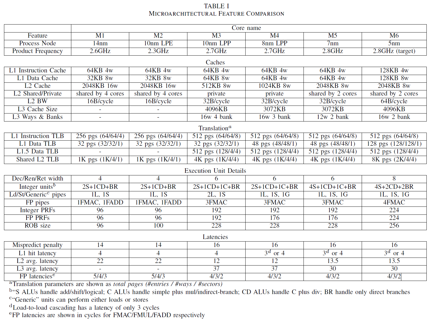
The disclosure covers some of the well-known characteristics of the design as had been disclosed by Samsung in its initial M1 CPU microarchitecture deep dive at HotChips 2016, to the more recent M3 deep dive at HotChips 2018. It gives us an insight into the new M4 and M5 microarchitectures that we had measured in our S10 and S20 reviews, as well as a glimpse of what the M6 would have been.
The one key characteristic of Samsung’s design was over the years, it was based off the same blueprint RTL that was started off with the M1 core in 2011, with continuous improvements of the functional blocks of the cores over the years. The M3 had been a big change in the design, widening the core substantially in several aspects, such as going from a 4-wide design to a 6-wide mid-core.
The new disclosures that weren’t public before regard the new M5 and M6 cores. For the M5, Samsung had made bigger changes to the cache hierarchy of the cores, such as replacing private L2 caches with a new bigger shared cache, as well as disclosing a change in the L3 structure from a 3-bank design to a 2-bank design with less latency.
The unreleased M6 core that had been in development was seemingly to be a bigger jump in terms of the microarchitecture. The SARC team here had prepared large improvements, such as doubling the L1 instruction and data caches from 64KB to 128KB – a design choice that’s currently only been implemented before by Apple’s CPU cores starting with the A12.
The L2 is said to have been doubled in its bandwidth capabilities to up to 64B/cycle, and also there would have been an increase in the L3 from 3 to 4MB.
The M6 would have been an 8-wide decode core, which as far as we know would have been the widest commercial microarchitecture that we know of – at least on the decode side of things.
Interestingly, even though the core would have been much wider, the integer execution units wouldn’t have changed all that much, just seeing one complex pipeline adding a second integer division capability, whilst the load/store pipelines would have remained the same as on the M5 with 1 load unit, 1 store unit, and one 1 load/store unit.
On the floating-point/SIMD pipelines we would have seen an additional fourth unit with FMAC capabilities.
The TLBs would have seen some large changes, such as the L1 DTLB being increased from 48 pages to 128 pages, and the main TLB doubling from 4K pages to 8K pages (32MB coverage).
The M6 would also have ben the first time since the M3 that the out-of-order window of the core would have been increased, with larger integer and floating-point physical register files, and an increase in the ROB (Reorder buffer) from 228 to 256.
One key weakness of the SARC cores seems to still have been present in the M5 and upcoming M6 core, and that’s its deeper pipelines stages resulting in a relatively expensive 16-cycle mispredict penalty, quite higher than Arm’s more recent designs which fall in at 11 cycles.
The paper goes into more depth into the branch predictor design, showcasing the core’s Scaled Hashed Perceptron based design. The design had been improved continuously over the years and implementations, improving the branch accuracy and thus reducing the MPKI (mis-predicts per kilo-instructions) continuously.
An interesting table that’s showcased is the amount of storage structures that the branch predictor takes up within the front-end, in KBytes:
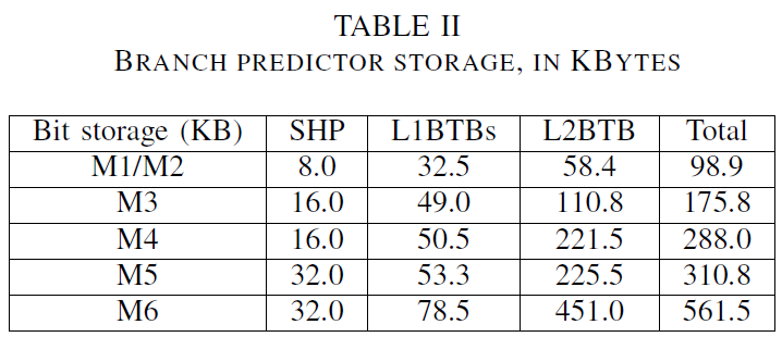
We’re not aware of any other vendor ever having disclosed such figures, so it’s interesting to put things into context of what a modern front-end has to house in terms of storage (and this is *just* the branch predictor).
The paper goes onto further detail onto the cores prefetching methodologies, covering the introduction of a µOP cache in the M5 generation, as well as the team’s efforts into hardening the core against security vulnerabilities such as Spectre.
Generational IPC Improvements - 20% per year - 2.71x in 6 years
The paper further describes efforts by the SARC team to improve memory latency over the generations. In the M4 core, the team had included a load-load cascade mechanism that reduced the effective L1 cycle latency from 4 cycles to 3 on subsequent loads. The M4 had also introduced a path bypass with a new interface from the CPU cores directly to the memory controllers, avoiding traffic through the interconnect, which explains some of the bigger latency improvements that we’ve seen in the Exynos 9820. The M5 had introduced speculative cache lookup bypasses, issuing a request to both the interconnect and the cache tags simultaneously, possibly saving on latency in case of a cache miss as the memory request is already underway. The average load latency had been continuously improved over the generations, from 14.9 cycles on the M1 down to 8.3 cycles on the M6.

In terms of IPC improvements, the SARC team had managed to get to an average of 20% annual improvements over the 8 years of development. The M3 had been in particular a big jump in IPC as seen in the graph. The M5 roughly correlates to what we’ve seen in our benchmarks, at around 15-17% improvement. IPC for the M6 is disclosed at having ended up at an average of 2.71 versus 1.06 for the M1, and the graph here generally seems to indicate a 20% improvement over the M5.
During the Q&A of the session, the paper’s presenter, Brian Grayson, had answered questions about the program’s cancellation. He had disclosed that the team had always been on-target and on-schedule with performance and efficiency improvements with each generation. It was stated that the team’s biggest difficulty was in terms of being extremely careful with future design changes, as the team never had the resources to completely start from scratch or completely rewrite a block. It was said that with hindsight, the team would have done different choices in the past with of some of the design directions. This serial design methodology comes in contrast to Arm’s position, having multiple leapfrogging design centres and CPU teams, allowing them to do things such as ground-up re-designs, such the Cortex-A76.
The team had plenty of ideas for improvements for upcoming cores such as the M7, but the decision to cancel the program was said to have come from very high up at Samsung. The SARC CPU cores were never really that competitive, suffering from diminished power efficiency, performance, and area usage compared to Arm’s designs. With Arm’s latest Cortex-X1 divulged last week going for all-out performance, it looks to me that SARC’s M6 design would have had issues competing against it.
The paper's authors are extremely thankful for Samsung’s graciousness in allowing the publication of the piece, and thank the SARC leadership for their management over the years on this “moonshot” CPU project. SARC currently still designs custom interconnects, memory controllers, as well as working on custom GPU architectures.
Related Reading:
- Arm's New Cortex-A78 and Cortex-X1 Microarchitectures: An Efficiency and Performance Divergence
- The Samsung Galaxy S20+, S20 Ultra Exynos & Snapdragon Review: Megalomania Devices
- The Samsung Galaxy S10+ Snapdragon & Exynos Review: Almost Perfect, Yet So Flawed
- Hot Chips 2018: Samsung’s Exynos-M3 CPU Architecture Deep Dive
- Hot Chips 2016: Exynos M1 Architecture Disclosed
Source: ISCA 2020: Evolution of the Samsung Exynos CPU Microarchitecture


51 Comments
View All Comments
melgross - Thursday, June 4, 2020 - link
The point is that Samsung g has a lot of experience and resources to do that. When Apple announced they were going to design their own, they were ridiculed for it. How would it be possible people asked? But they did it. Samsung could have made the decision to do this the right way, if they wanted to. Asian companies are very conservative. They aren’t willing to take the chances that others do, particularly American companies.So Samsung became nervous over the prospect, and chickened out. That what it was.
dotjaz - Friday, June 5, 2020 - link
They took a chance and failed miserably, they are not the only one. Qualcomm failed miserably as well.dotjaz - Wednesday, June 3, 2020 - link
Also funny you should mention Qualcomm and server cores, remember the hugely successful Centriq? I don't think so.Both Amazon and Ampere as well as EPI have switched to Neoverse. The only ones left standing (for now) are Marvell and HiSilicon. And based on current market share and performance, neither are that promising.
eastcoast_pete - Wednesday, June 3, 2020 - link
I believe for the chance to be the king of the performance hill for Android (and maybe Windows on ARM), with performance similar to Apple's big cores. But yes, that didn't exactly happen. However, sometimes you have to invest at risk if you're after big rewards.melgross - Thursday, June 4, 2020 - link
Maybe you don’t. I understand it very well. Samsung Electronics is a company with over $200 billion in sales. You apparently don’t know that. They spend close to $20 billion a year on R&D. I guess you don’t know that either. If they really wanted to selol their SoCs to others, the way they did to Apple for a few years, they needed to up their game. Apple was, according to reports, 40% of their SoC production in dollars. That was a major loss, and shook the company. The fact is that they went the wrong way with their designs. They needed to, as they admitted, redesign a fair amount of it from scratch.They could have done that if they decided to spend just a bit more. But upper management decided instead to retrench, and give up on the possibility of really competing with Qualcomm and others. We’ll never know what could have happened now. This presentation was that of a failed design, nothing more.
anonomouse - Wednesday, June 3, 2020 - link
It's not like they had infinite engineers they could go hire even if they wanted to, and adding more engineers doesn't mean a linear increase in productivity either. They made it clear how important schedule was for them. An aggressive yearly update cadence certainly would have made large, ambitious changes or clean reimplementations quite risky. It's like they said, they couldn't ever afford to miss the product schedule for the phone, so they probably just ended up stuck with a bunch of suboptimal early choices that they couldn't really fix. I mean, look at size, width and depth they're talking about in M6 and compare that with similar or worse performance wrt A77, which is much smaller, narrower, and shallower. Or compare to Apple, which doesn't explicitly disclose any of these things, but there are no clearly indications that it is substantially larger in any particular dimension (except caching in the further parts of the memory subsystem), and yet has vastly superior IPC. Clearly there must be a lot of issues all over the place that they just never could get around to fixing.WJMazepas - Wednesday, June 3, 2020 - link
What i dont get it is why Samsung invested in the M Cores. They didnt funded they enough. Was not better then just license the ARM IP? It probably would be cheaperjeremyshaw - Wednesday, June 3, 2020 - link
When they started, just about everyone that mattered was still running their own custom uarch. Apple, Nvidia, Qualcomm, etc. Of the big Cortex-A customers of that era: Mediatek wasn't a threat, Broadcom would never really enter the mobile market, and TI would withdraw from application processors altogether. From the picture of when Samsung started, custom cores were the way to go. Since then, Nvidia has constantly wavered on custom cores vs Cortex-A, Qualcomm has went to using optioned out Cortex-A cores, TI is still gone, Broadcom never even sniffed the market again, and Mediatek is still Mediatek. All the while, Apple's yearly CPU gains were slowing down and Cortex-A were getting a lot better.The picture just wasn't so clear back then.
Samsung also had a chance to basically hire away one of AMD's "small core" teams (specifically the one which designed the Xbox One and PS4's CPU uarch), though that didn't pan out.
lmcd - Thursday, June 4, 2020 - link
Nvidia wavering on custom vs not is irrelevant considering they entirely left the consumer portable device market. They couldn't get either in a low enough power profile at the performance they deemed acceptable.Qualcomm didn't choose to go to Cortex, they fucked up their aarch64 core design so badly that they scrapped it. Someone higher up realized that they could just coast on their modems, so they did.
Broadcom didn't even matter back then so idk what you're referencing. They had 3-5 random design wins total and most were $0-on-contract type devices. Their lineup didn't have up-to-date graphics and they never used a higher-end CPU core.
Quite frankly, Samsung should've gone a more extreme route than they did if they wanted a custom SoC: get an exclusive license to AMD's cat cores in mobile, and integrate them into a Samsung SoC. Tablets were still the rage back then, so you could pawn off the first few iterations on Android tablets. A Jaguar core, die-shrunk, would be solid as a smartphone CPU core even right now.
brucethemoose - Wednesday, June 3, 2020 - link
Well theres a good lesson: deeper, longer term investments yield proportionally more competitive products.I get that Samsung "needed" a new uarch for every Galaxy, but in hindsight, they should've the bullet every other year.