Samsung Announces "X-Cube" 3D TSV SRAM-Logic Die Stacking Technology
by Andrei Frumusanu on August 14, 2020 7:00 AM EST- Posted in
- Samsung Foundry
- TSV
- Packaging
- 3D Packaging
Yesterday, Samsung Electronics had announced a new 3D IC packaging technology called eXtended-Cube, or “X-Cube”, allowing chip-stacking of SRAM dies on top of a base logic die through TSVs.
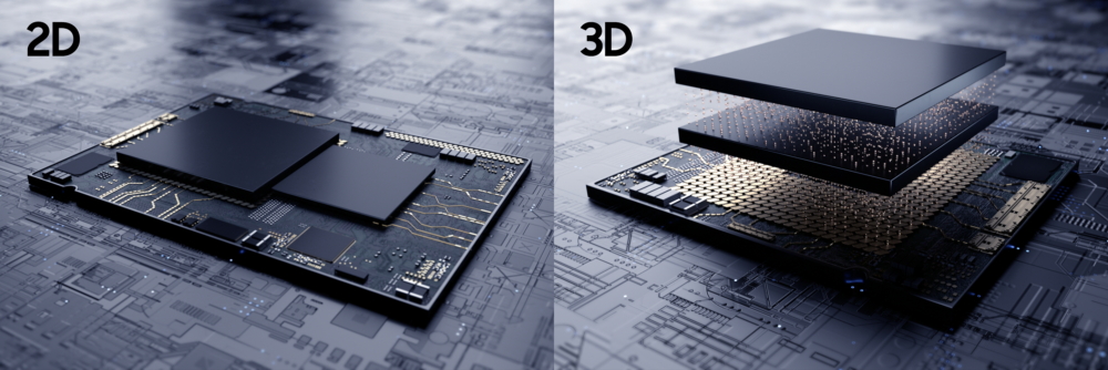
Current TSV deployments in the industry mostly come in the form of stacking memory dies on top of a memory controller die in high-bandwidth-memory (HBM) modules that are then integrated with more complex packaging technologies, such as silicon interposers, which we see in today’s high-end GPUs and FPGAs, or through other complex packaging such as Intel’s EMIB.

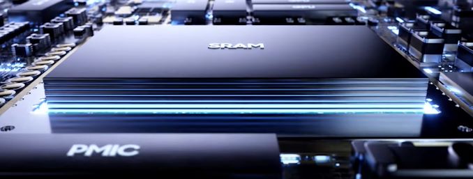
Samsung’s X-Cube is quite different to these existing technologies in that it does away with intermediary interposers or silicon bridges, and directly connects a stacked chip on top of the primary logic die of a design.
Samsung has built a 7nm EUV test chip using this methodology by integrating an SRAM die on top of a logic die. The logic die is designed with TSV pillars which then connect to µ-bumps with only 30µm pitch, allowing the SRAM-die to be directly connected to the main die without intermediary mediums. The company this is the industry’s first design such design with an advanced process node technology.
It’s not the first time that the company has demonstrated TSVs in the base logic die to connect to a stacked die on top of it. Back in 2013, the company had showed custom Exynos chips using Widcon technology, stacking Wide I/O DRAM memory on top of the base logic chip with help of TSVs, offering a higher-performance and lower power solution compared to traditional PoP memory. Unfortunately, this technology never saw the light of day in consumer devices as it likely never was cost-effective enough justify for mass-production.
Stacking more valuable SRAM instead of DRAM on top of the logic chip would likely represent a higher value proposition and return-on-investment to chip designers, as this would allow smaller die footprints for the base logic dies, with larger SRAM cache structures being able to reside on the stacked die. Such a large SRAM die would naturally also allow for significantly more SRAM that would allow for higher performance and lower power usage for a chip.
Samsung’s marketing materials showcase more than a single die of SRAM, which would indicate that X-Cube can be variable in terms of its stack-height. It’s currently unclear if X-Cube will be limited to SRAM dies, or whether it will also extend to future logic-over-logic stacking.
Samsung is providing silicon proven design methodology and flow for its advanced 7nm and 5nm nodes, and states that X-Cube will be utilised for advanced applications such as mobile, AR/VR, wearable and HPC designs. The company is also planning a presentation on X-Cube at Hot Chips this Sunday where it will revealing more details on the technology.


20 Comments
View All Comments
nandnandnand - Friday, August 14, 2020 - link
I'm waiting for those giant L4 caches to start appearing, like gigabytes of DRAM stacked on the I/O die with AMD Zen 4/5, or Intel's Foveros. Maybe if you buy a more expensive CPU, you'll get a larger L4 cache in addition to the higher core count.dwillmore - Friday, August 14, 2020 - link
"The company this is the industry’s first design such design with an advanced process node technology."I think you're missing a verb there in the beginning of that sentence.
dwillmore - Monday, August 17, 2020 - link
So, articles here are just throwaway? Post and forget, huh? No reading the comments--not even for spam let alone corrections.zamroni - Friday, August 14, 2020 - link
When will sram replace dram?Based on transistor count, sram price should be 6x of dram. So, it quite economical for server use case
ksec - Friday, August 14, 2020 - link
What about heat and cooling?How is that going to work?
Kamen Rider Blade - Friday, August 14, 2020 - link
I could be wrong about this, but the SRAM portions on a CPU don't get nearly as hot as the Compute/Switching portions. Ergo, there should be a bit more room for Heat in the SRAM areas such as L1/L2/L3 $.Kamen Rider Blade - Friday, August 14, 2020 - link
I think the more important use for this is for SMT (Simultaneous Multi-Threading)Imagine SMT4, SMT8, each thread with it's own SRAM layer.
Ergo help preventing Threads from peaking into other threads via physical isolation for security and allowing fast swapping of Threads because each Thread would be loaded already for the Registers to use.
No need to flush out L1D$ or L1I$ as you can literally swap to a different thread and do work on that Thread/layer's L1D$ or L1$. That saves you a few steps in the CPU cycle.
Or if you have to flush, a different part of the CPU that is dedicated to loading L1$ can operate while the main registers are busy, ergo minimizing idle-time.
pixelstuff - Friday, August 14, 2020 - link
E-Cube would have been better.Diogene7 - Saturday, August 15, 2020 - link
I am wondering if Samsung X-Cube technology is or could be compatible with STT-MRAM (or even better, SOT-MRAM) to get several Megabytes or maybe even Gigabytes of fast non-volatile memory close to the CPU : it would be quite disrupting compare to what exist as of 2020, and open plenty of new opportunities (especially to create low-power always-on devices)silencer12 - Sunday, August 16, 2020 - link
So since HBM was designed and went up against Micron's memory-cube. Is Samsung doing a more improved version due to Micron's technology failing to become adopted?That's what it appears