‘Better Yield on 5nm than 7nm’: TSMC Update on Defect Rates for N5
by Dr. Ian Cutress on August 25, 2020 9:30 AM EST
One of the key metrics on how well a semiconductor process is developing is looking at its quantitative chip yield – or rather, its defect density. A manufacturing process that has fewer defects per given unit area will produce more known good silicon than one that has more defects, and the goal of any foundry process is to minimize that defect rate over time. This will give the customers better throughput when making orders, and the foundry aims to balance that with the cost of improving the manufacturing process.
The measure used for defect density is the number of defects per square centimeter. Anything below 0.5/cm2 is usually a good metric, and we’ve seen TSMC pull some really interesting numbers, such as 0.09 defects per square centimetre on its N7 process node only three quarters after high volume manufacturing started, as was announced in November at the VLSI Symposium 2019. As it stands, the defect rate of a new process node is often compared to what the defect rate was for the previous node at the same time in development. As a result, we got this graph from TSMC’s Technology Symposium this week:
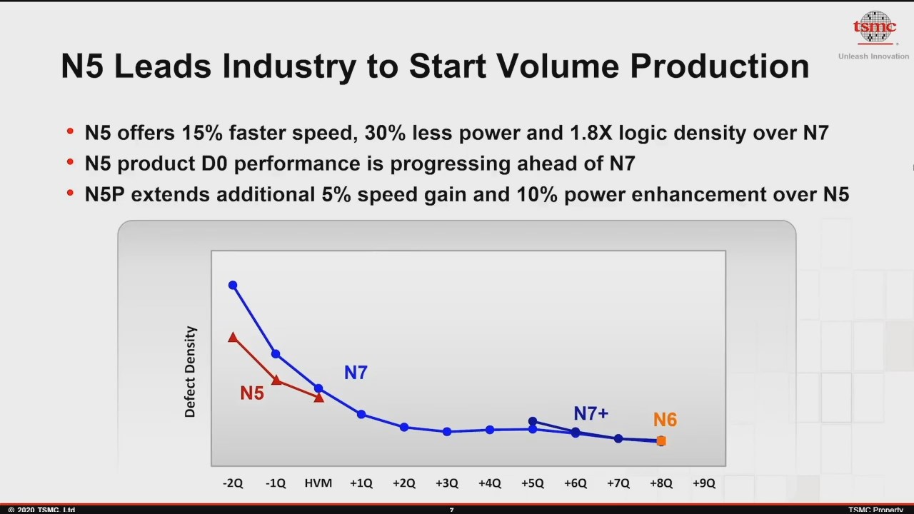
As it stands, the current N5 process from TSMC has a lower defect density than N7 did at the same time in its development cycle. TSMC. This slide from TSMC was showcased near the start of the event, and a more detailed graph was given later in the day:
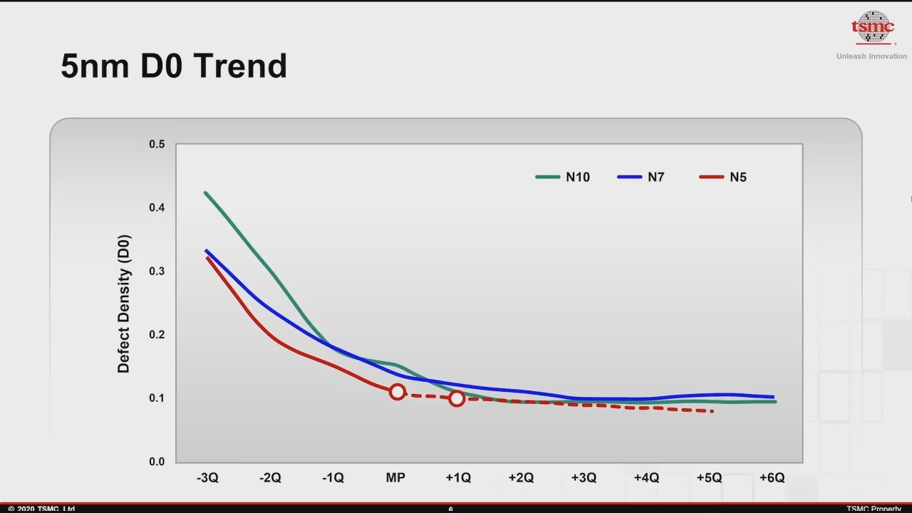
This plot is linear, rather than the logarithmic curve of the first plot. This means that TSMC’s N5 process currently sits around 0.10 to 0.11 defects per square centimeter, and the company expects to go below 0.10 as high volume manufacturing ramps into next quarter.
Part of what makes 5nm yield slightly better is perhaps down to the increasing use of Extreme UltraViolet (EUV) technology, which reduces the total number of manufacturing steps. Each step is a potential chance to decrease yield, so by replacing 4 steps of DUV for 1 step of EUV, it eliminates some of that defect rate.
TSMC’s first 5nm process, called N5, is currently in high volume production. The first products built on N5 are expected to be smartphone processors for handsets due later this year.
Related Reading
- TSMC Details 3nm Process Technology: Full Node Scaling for 2H22 Volume Production
- TSMC To Build 5nm Fab In Arizona, Set To Come Online In 2024
- TSMC & Broadcom Develop 1,700 mm2 CoWoS Interposer: 2X Larger Than Reticles
- TSMC Boosts CapEx by $1 Billion, Expects N5 Node to Be Major Success
- Early TSMC 5nm Test Chip Yields 80%, HVM Coming in H1 2020
- TSMC: 5nm on Track for Q2 2020 HVM, Will Ramp Faster Than 7nm
- TSMC: N7+ EUV Process Technology in High Volume, 6nm (N6) Coming Soon


102 Comments
View All Comments
tuxRoller - Friday, August 28, 2020 - link
That wiki chip link mentions that tsmc focused on hpc for the first 5nm iteration rather than their usual LP. That may account for the difference in defect rates between 7 & 5.martixy - Sunday, August 30, 2020 - link
So... good things are coming in 2021, is what I'm reading here.