3DFabric: The Home for TSMC’s 2.5D and 3D Stacking Roadmap
by Dr. Ian Cutress on September 2, 2020 11:00 AM EST
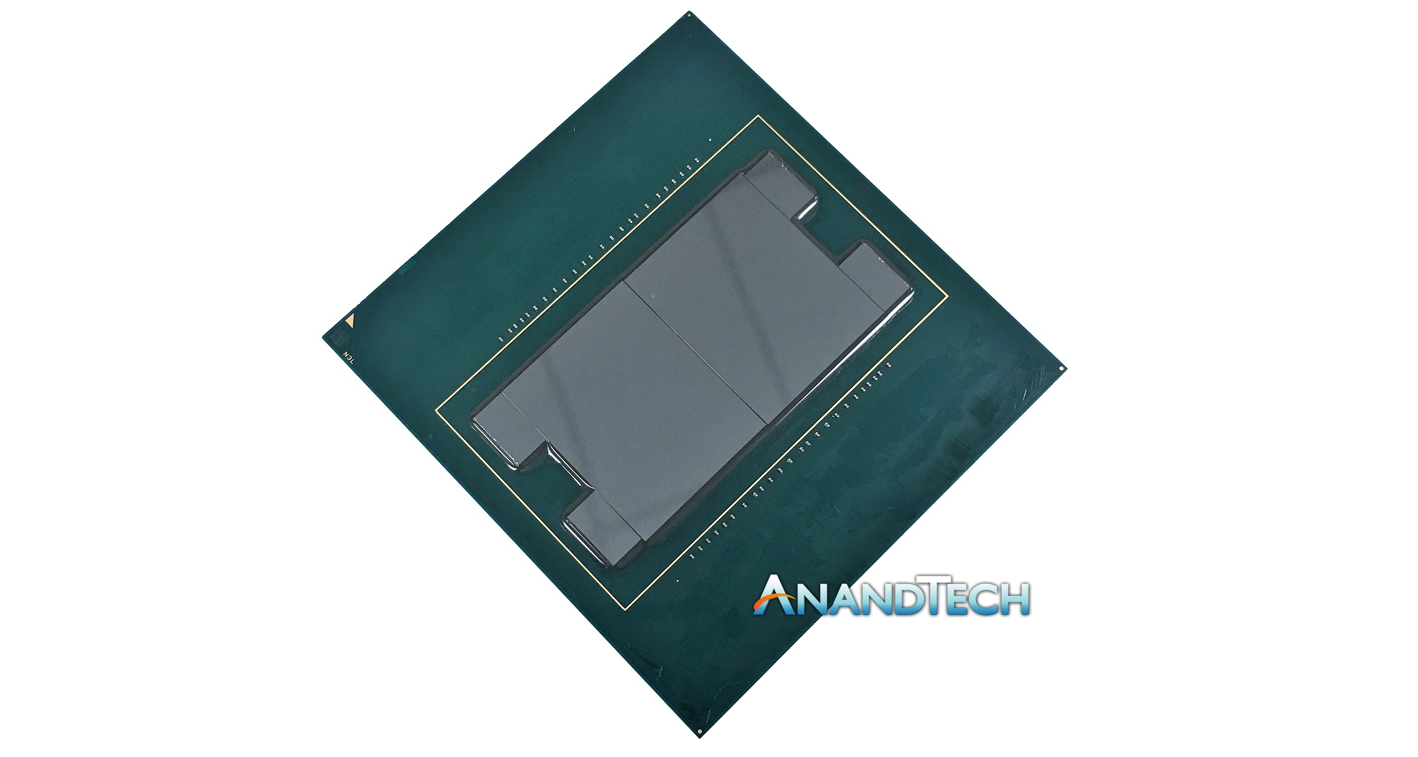
Interposers. EMIB. Foveros. Die-to-die stacking. ODI. AIB. TSVs. All these words and acronyms have one overriding feature – they are all involved in how two bits of silicon physically connect to each other. At the simple level, two chips can be connected through the printed circuit board – this is cheap but doesn’t allow for great bandwidth. Above this simple implementation, there are a variety of ways to connect multiple chiplets together, and TSMC has a number of these technologies. In order to unify all the different names it gives to its variants of its 2.5D and 3D packaging, TSMC has introduced its new overriding brand: 3DFabric.
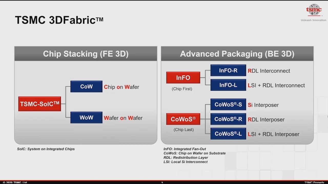
3DFabric makes sense as a brand to tie the dozen or so combinations of packaging technology that TSMC offers. Broadly speaking, 3DFabric is split into two segments: on one side are all the ‘front-end’ chip stacking technologies, such as chip-on-wafer, while the other side is the ‘back-end’ packaging technologies such as InFO (Integrated Fan-Out) and CoWoS (Chip-On-Wafer-On-Substrate).
Even with this arrangement of TSMC’s technologies, it still introduces a lot of acronyms for users not familiar with packaging offerings. Some of them aren’t always obvious either, such as RDL or LSI, especially for those that are used to Intel’s brand names for the packaging technologies it has. Hopefully we can deconstruct what these terms and compare them to offerings at other foundries.
TSMC-SoIC: Front-End Chip Stacking
The front-end chip stacking technologies, such as chip-on-wafer and wafer-on-wafer, are collectively known as ‘SoIC’, or System of Integrated Chips. The goal of these technologies is to stack bits of silicon on top of each other without using the ‘bumps’ that we see on the back-end integration options. Here, the SoIC designs are literally creating bonding interfaces such that silicon can sit on top of silicon, as if it was a single piece of silicon to begin with.
This is a technically more complex procedure, and the benefits often lie in thermal performance:
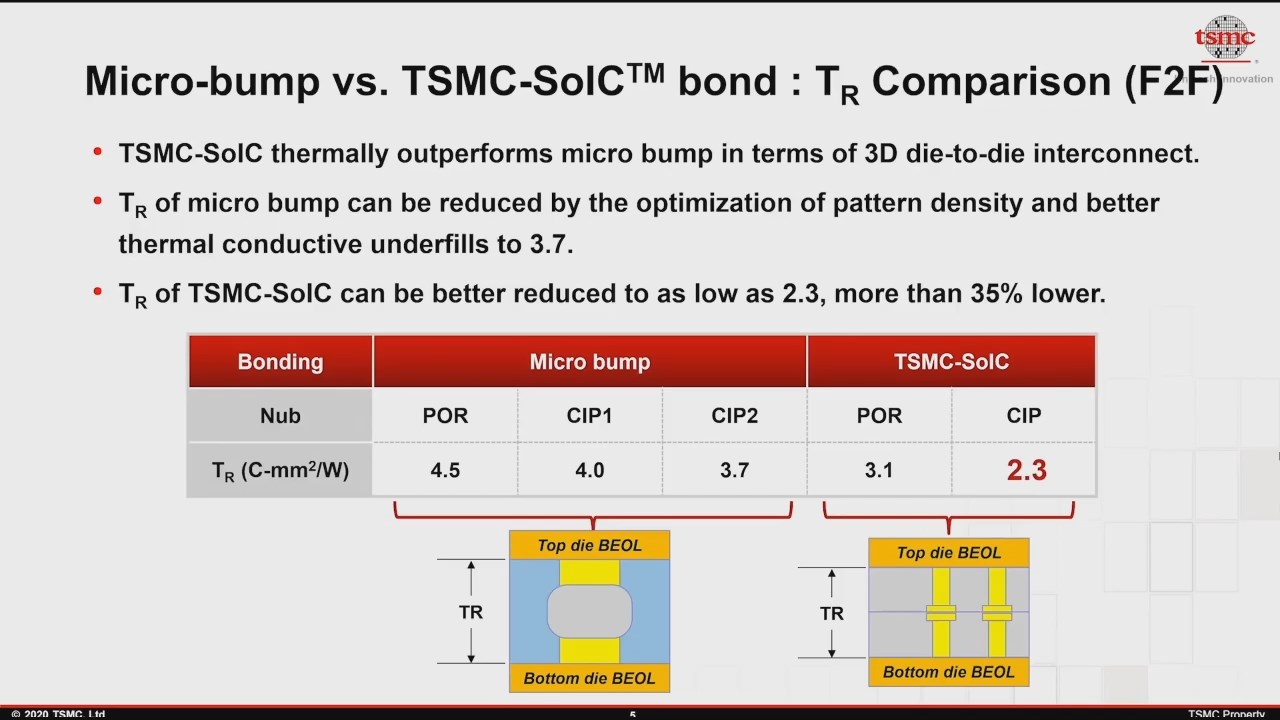
This slide shows that the thermal resistance of a face-to-face SoIC bond is up to 35% lower than a micro-bump connection, and as we move into the future of compute with multiple packaged chips, managing those interfaces for thermals is going to be tough. The downside of these SoIC technologies however is that the stacked design has to be co-designed with each other – microbump technologies, such as EMIB, are done in such a way that technically a range of chips could be connected together. Using SoIC, as chip-on-wafer or wafer-on-wafer, the designs are fixed in from the start.

Nonetheless, TSMC is keen to promote its SoIC chip stacking abilities, with a demonstration of a 12-layer stack as part of the slide deck. You can read our separate coverage of this in our news article.
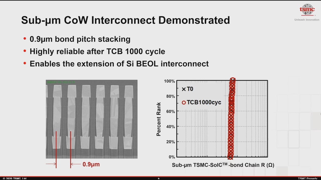
Naturally there is concern about connecting two bits of silicon without micro-bumps, such as density and reliability. TSMC states that they can demonstrate reliable 0.9 micron bond pitches in a very reliable format. If we compare that to the best bump pitch stacking that Intel has on its roadmap, the company is aiming for 10-micron bump pitches, which is an order of magnitude higher. In this case, for the chips where it makes sense, SoIC offers better connectivity density and lower energy-per-bit.
TSMC is planning to offer SoIC options on its N7, N5, and N3 process nodes, with the TSV pitches scaling down from 9 micron to 4.5 micron in that time. TSMC is expecting a regular cadence to this release schedule, with options appearing approximately 6-12 months after each respective node moves into high volume manufacturing.
TSMC Back-End Advanced Packaging
Competing against EMIB and Foveros
The other element in packaging is the simpler end of the spectrum: connecting two silicon die on a single package. This is usually done with the two pieces of silicon side-to-side, with a variety of ways for connection.
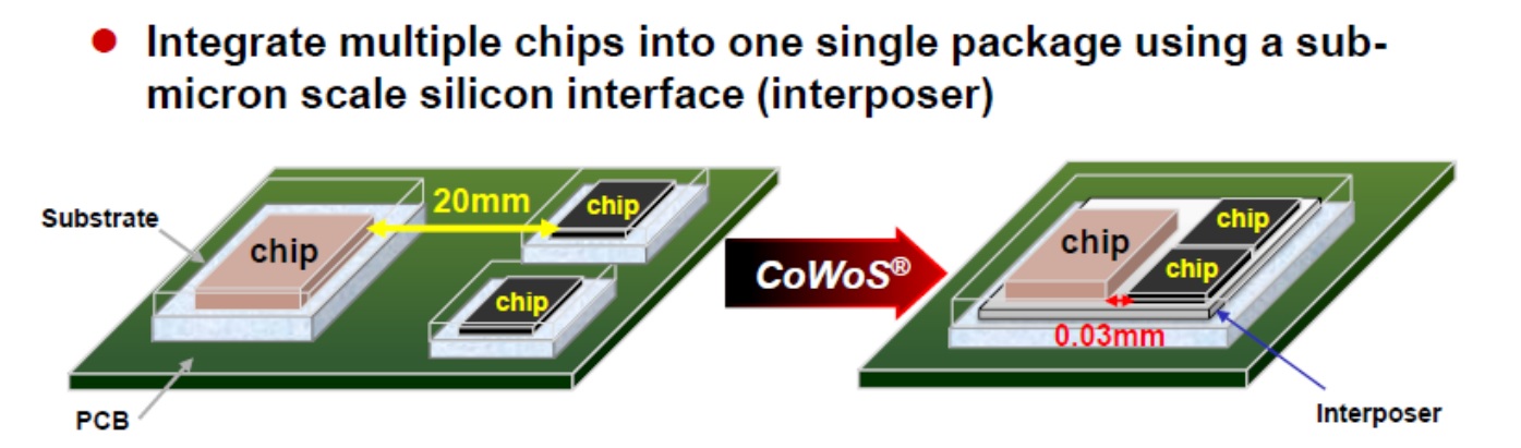
The one that most people are familiar with is the interposer method, where a large piece of silicon sits underneath all the interconnected dies, and acts as a faster routing method than simply laying traces through a PCB package.

NEC SX-Aurora TSUBASA with 6 HBM2 Stacks
The other method is, in similar terms, interposer technology, however the interposer is embedded in the PCB and is only used to connect one specific die to another (this is what Intel calls its Embedded Multi-Die Interconnect Bridge, or EMIB).
Intel's equivalent EMIB solution
The third is direct die-on-die vertical stacking, however this is different to the SoIC implementations mentioned above due to the use of micro-bumps between the two pieces of silicon, whereas SoIC uses bonding. In fact, all of the implementations in this second half of TSMC’s offerings are micro-bump based – this allows for better mix and match scenarios between different chips after each chip is made, however it doesn’t get the benefits of density or power that SoIC provides.
This is why it’s called ‘back-end’ advanced packaging – take for example, a HBM-enabled GPU.
A number of HBM-enabled GPUs have a single GPU die, several HBM die, all placed on top of an interposer. The GPU and HBM are made by different companies (and even different HBM could be used), while the silicon interposer can also be made elsewhere. This silicon interposer can be passive (contain no logic, only die-to-die routing), or it can be active, and designed to be a better network interconnect between chips if required, although this means the interposer would consume power.
TSMC’s GPU-like interposer strategy has historically been called CoWoS – chip-on-wafer-on-substrate. As part of 3DFabric, CoWoS now has three variants depending on the type of implementation.
The standard one everyone is familiar with is being called CoWoS-S, where S stands for Silicon Interposer. The limit of CoWoS-S is all in the size of the interposer, which is often built on a 65nm manufacturing process or similar. As the interposer is a single piece of silicon, it has to be manufactured similarly, and as we move into a chiplet era, customers are asking for bigger and bigger interposers, which means TSMC has to be able to manufacture them (and give high yield). Traditional chips are limited by what is known as the size of the reticle, which is a fundamental limit inside of a machine as to how big it can ‘print’ a layer at a single instance. In order to enable products whose chips are on the reticle size, TSMC has been developing multi-reticle sized interposer technology, allowing these products to be big. Based on TSMC’s own roadmaps, we are expecting CoWoS implementations in 2023 to be around 4x the size of the reticle, allowing for over 3000+ mm2 of active logic silicon per product. We have a news item specifically covering this technology that you can read here.

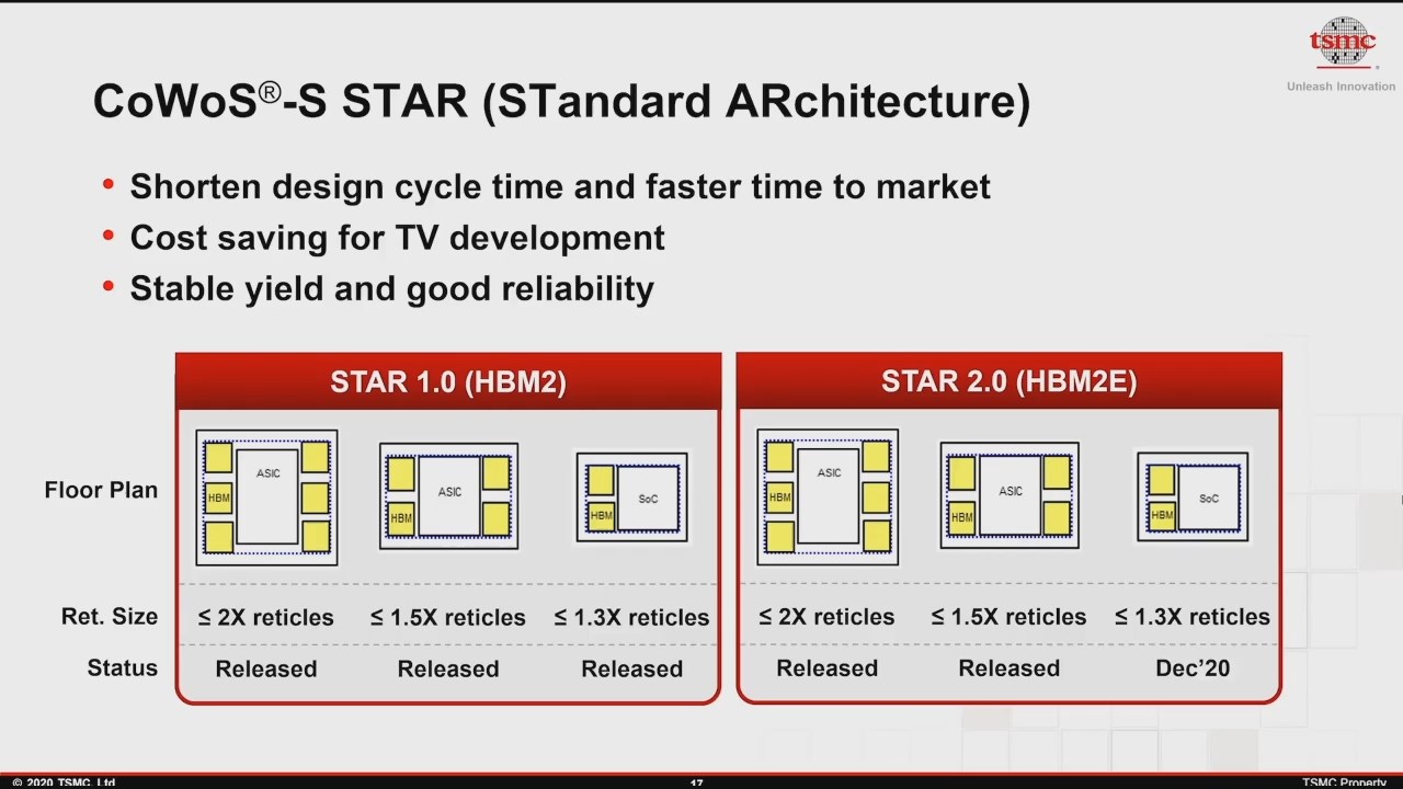
Due to CoWoS-S being a popular implementation for the ASIC+HBM crowd, TSMC is also implementing a technology track called CoWoS-S STAR, for STandard ARchitecture. This will allow customers to work within specific design protocols for 2/4/6 HBM stacks, minimize the size of the interposer, but also speed up time to market and improve yield.
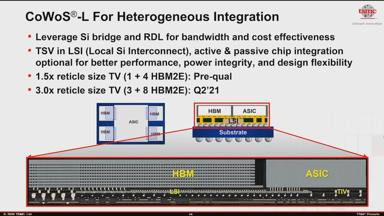
CoWoS-L is another variant, using local silicon interconnects and a redistribution layer. The key word here is ‘local’, meaning that it connects two silicon die together locally. This is going to be TSMC’s approach to Intel’s EMIB. While Intel’s EMIB is already in use for several products (Kaby-G, Stratix 10, Agilex FPGA), TSMC is only currently in pre-qualification right now. The way TSMC seem to be implementing CoWoS-L is by placing all of the bridge interconnects onto a package at once, and so the technology is limited by the furthest distances away from each of the interconnects. As in the slide below, TSMC is aiming for 3.0x reticle for CoWoS-L in Q2 2021.
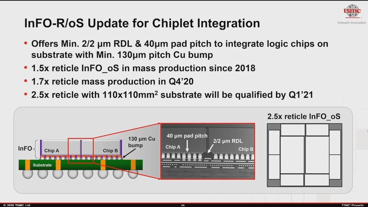
InFO (Integrated Fan Out) packaging allows chips to ‘fan out’ additional connections outside the standard floorplan of an SoC. This means that while a chip logic area can be small, the chip is made bigger than the logic to accommodate all the required pin-out connections. TSMC has been offering InFO for a number of years, however under 3DFabric it will now offer different types of InFO related to in-package connectivity.
InFO-R (also known as InFO_oS) allows for a redistribution layer to be added between the die and the microbumps in order to unify multiple die into a single package. This is another technique whereby the limiting factor is the x/y dimensions of the technology, measured in reticle sizes. Currently TSMC supports InFO-R at 1.5x reticle since 2018, and will move to 1.7x reticle in Q4 2020 with 2.5x reticle by Q1 2021.
InFO-L is similar to CoWoS-L in that it uses a localized silicon interconnect to connect multiple InFO dies together. This technology is still a work in progress, with qualification expect to complete in Q1 2021.

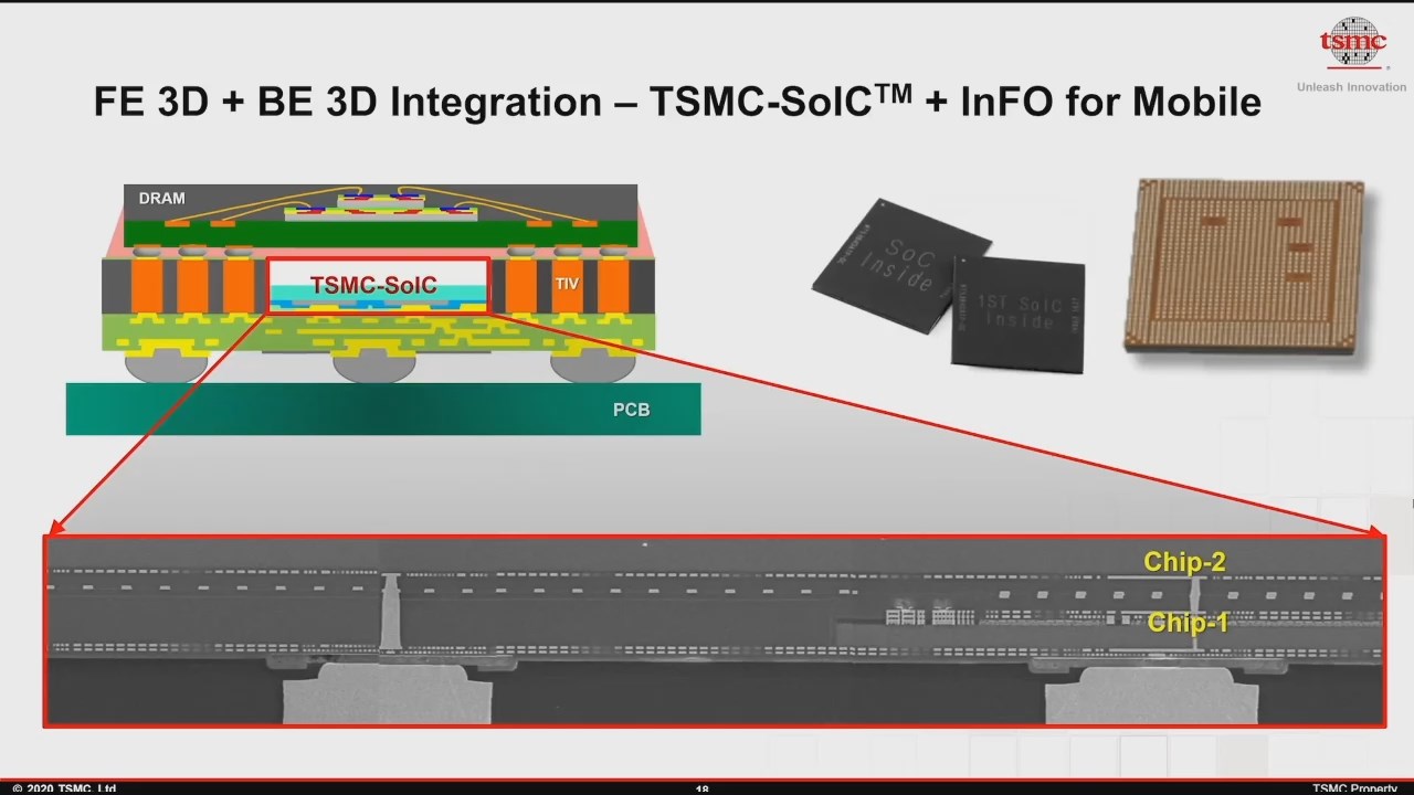
TMSC’s packaging technologies can also be combined in the same product. By implementing both front end (SoIC) and back-end (InFO) packaging, new classes of products can be made. The company produced one such mock-up:
On the face of it, TSMC looks set to offer more packaging options for its customers over the coming years. The main competition on this seems to be Intel, who has been able to implement its EMIB and Foveros technologies in a few current products and some to-be-released products. TSMC will have the benefit of working with more projects and customers to help deliver these technologies, in a way that Intel might struggle with. I will hand it to Intel however, the marketing for its technologies is a lot easier to remember. The minute someone says EMIB or Foveros, I know exactly what they’re talking about – with TSMC, just saying ‘3DFabric’ could mean a lot of things, SoIC is pretty clear, but then differentiating between CoWoS-S and CoWoS-L just doesn’t roll off the tongue as easily, and requires another mental step in order to make the connection.
Related Reading
- TSMC: N7+ EUV Process Technology in High Volume, 6nm (N6) Coming Soon
- TSMC: 3nm EUV Development Progress Going Well, Early Customers Engaged
- TSMC’s 5nm EUV Making Progress: PDK, DRM, EDA Tools, 3rd Party IP Ready
- ASML’s First Multi-Beam Inspection Tool for 5nm
- TSMC Expects 5nm to be 11% of 2020 Wafer Production (sub 16nm)
- ‘Better Yield on 5nm than 7nm’: TSMC Update on Defect Rates for N5
- TSMC Details 3nm Process Technology: Full Node Scaling for 2H22 Volume Production
- TSMC Confirms Halt to Huawei Shipments In September


9 Comments
View All Comments