Intel Launches 10nm Atom Embedded CPUs: Elkhart Lake Now Available
by Dr. Ian Cutress on September 23, 2020 9:00 AM EST
The embedded and edge markets for Intel have always been hidden away within its IoT business, however at the Investor Meeting last year it was highlighted as one of Intel’s key growth areas. The requirements for businesses to enable automation and control, as well as apply machine learning or computer vision, have increased as new optimized algorithms and use cases enter the market, and this is the question that the new 10nm Atom Embedded CPUs are set to answer.
Elkhart Lake built upon Tremont with 10nm
The new processors built with Tremont Atom cores will come as three series of processors: Pentium, Celeron, and Atom x6000E. These are all built with the same silicon die, offering up to four Atom cores with a 3.0 GHz turbo frequency, up to 850 MHz of Gen11 graphics (up to 32 EUs, three 4K60 displays), in TDPs ranging from 4.5 W to 12 W. All processors will support up to LPDDR4X-4267 or DDR4-3200. In-band ECC support is split - the Atom x6000E parts have it, but the Pentium and Celerons do not.
| Intel Elkhart Lake Tremont Atoms for Embedded |
||||||||
| AnandTech | Cores | Base MHz |
Turbo MHz |
GPU Base |
GPU MHz |
TDP |
TCC | TSI |
| Pentium J/N and Celeron J/N | ||||||||
| Pentium J6425 | 4 | 1800 | 3000 | 400 | 850 | 10W | - | - |
| Celeron J6413 | 4 | 1800 | 3000 | 400 | 800 | 10W | - | - |
| Pentium N6415 | 4 | 1200 | 3000 | 350 | 800 | 6.5W | - | - |
| Celeron N6211 | 2 | 1200 | 3000 | 250 | 750 | 6.5W | - | - |
| Atom x6000E | ||||||||
| Atom x6425E | 4 | 1800 | 3000 | 500 | 750 | 12W | - | - |
| Atom x6413E | 4 | 1500 | 3000 | 500 | 750 | 9W | - | - |
| Atom x6211E | 2 | 1200 | 3000 | 350 | 750 | 6W | - | - |
| Atom x6000RE: RTOS Support | ||||||||
| Atom x6425RE | 4 | 1900 | - | 400 | - | 12W | Yes | - |
| Atom x6414RE | 4 | 1500 | - | 400 | - | 9W | Yes | - |
| Atom x6212RE | 2 | 1200 | - | 350 | - | 6W | Yes | - |
| Atom x6000FE: Intel Safety Island Support | ||||||||
| Atom x6427FE | 4 | 1900 | - | 400 | - | 12W | Yes | Yes |
| Atom x6200FE* | 2 | 1000 | - | - | - | 4.5W | Yes | Yes |
| * Has no IGP | ||||||||
Intel is also moving to 10nm SuperFin (formerly 10++) for its Atom nodes, making these the next 10nm-class Atom processors after Intel’s Snow Ridge for 5G networks.
Intel has since updated and told us that these products use the same 10nm process as Ice Lake.
Focusing on IoT Features
Previous embedded processors like this were perhaps not always focused with the Edge market or the IoT market in mind. This time around however, Intel states that these products have been built from the ground up with this market in mind. This lends itself to a number of IoT-specific features.
There is now a new Programmable Services Engine to offload IoT workloads. This is a dedicated ARM processor, specifically an Arm Cortex M7, that supports real-time functionality, network synchronization, time sensitive networking, and low compute requirement workloads without needing to fire up the bigger cores. Some of the models support Time Coordinated Computing to enable worst-case execution time (WCET) and ultra-reliable low-latency communication (URLLC)
Two processors, the Atom x6427FE and x6200FE, are FuSa certified and support Intel’s Safety Island technology to allow integrated functional safety within IP blocks for finding and flagging faults, as well as initiating internal diagnostic tests.
All of these CPUs have three integrated 2.5 GbE MACs, all of which can be enabled for time-sensitive networking. The cores have Intel’s SHA extensions, as well as AES-NI and Intel Secure Key. Note that Intel is the only x86 vendors who does not have SHA-acceleration hardware, instead deciding to rely on instruction-level optimization.
The new processors all support Intel’s OpenVINO toolkit, with pre-optimized libraries for AI, ML, and computer vision acceleration. This is on top of Intel’s new Edge Software Hub, an interface for OEM customers to acquire pre-optimized deployment-ready software packages optimized for Industrial, Retail and Vision, all of which also offer customizability.
OS support is listed as Windows 10 IoT Enterprise, Yocto Project BSP, Linux Ubuntu, Wind River Linux LTS, and Android 10. The boot firmware supports Intel Slim Bootloader as well as coreboot, and the Programmable Services Engine runes on Intel’s own Zephyr RTOS-based platform.
For performance, Intel is claiming 1.7x single thread over two-generation old Apollo Lake Atoms, and 1.5x in multi-threaded workloads. Graphics performance gen-on-gen is listed as 2x. These numbers come from SPEC2006int and 3DMark11, but are based on pre-silicon projections of the new hardware (and it seems odd it wasn't compared to the Gemini Lake hardware). This would suggest that Intel doesn’t have the silicon in the labs yet to run the tests, which is a little odd if this is the launch day. Nonetheless, these platforms have a 7+ year lifecycle.
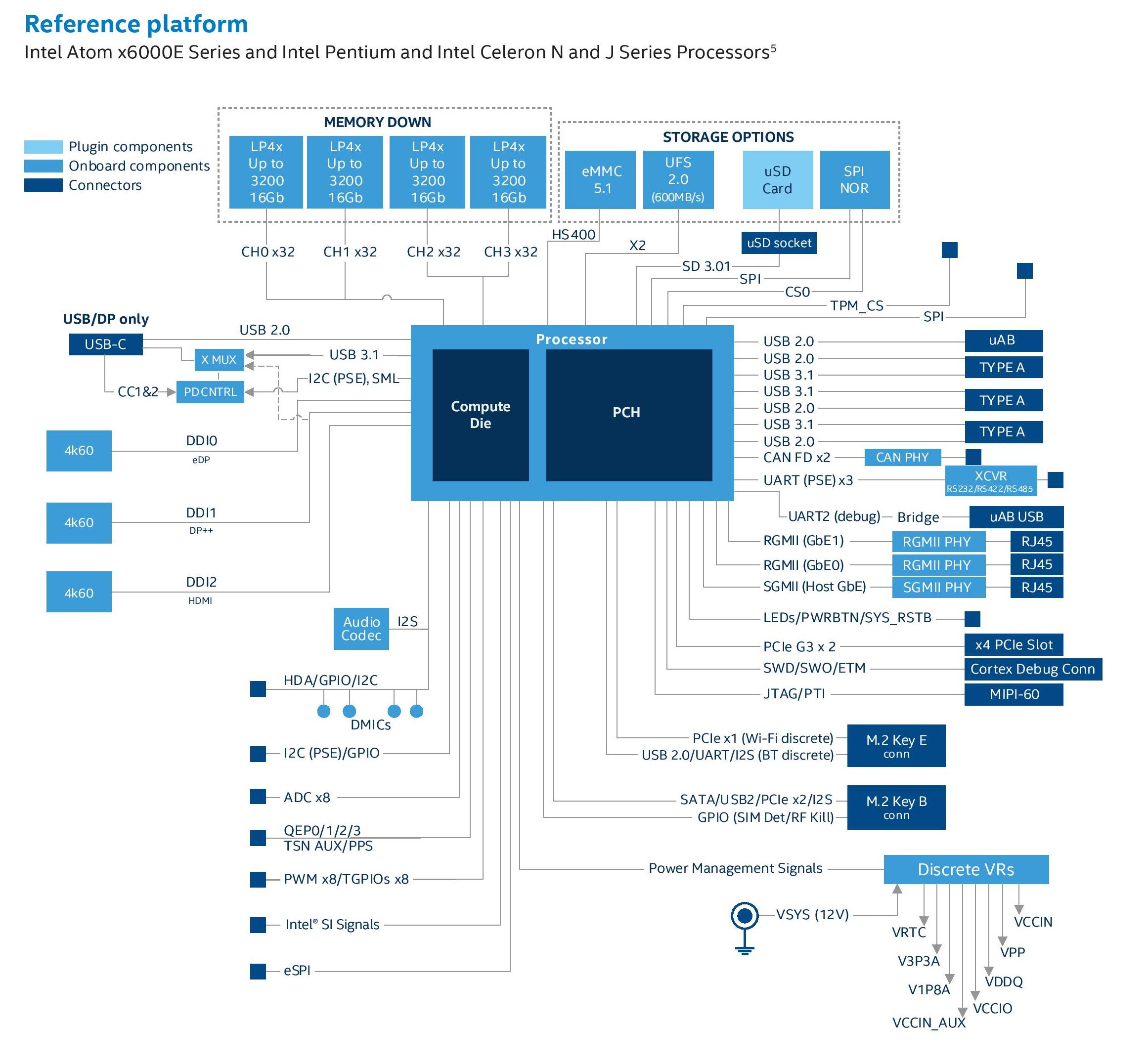
Click to zoom
Intel confirmed that the CPU-to-PCH connection is not DMI in this instance, but just OPIO. The chipset will support eight lanes of PCIe 3.0, four USB 3.1 ports, ten USB 2.0 ports, and two UFS 2.0 ports.
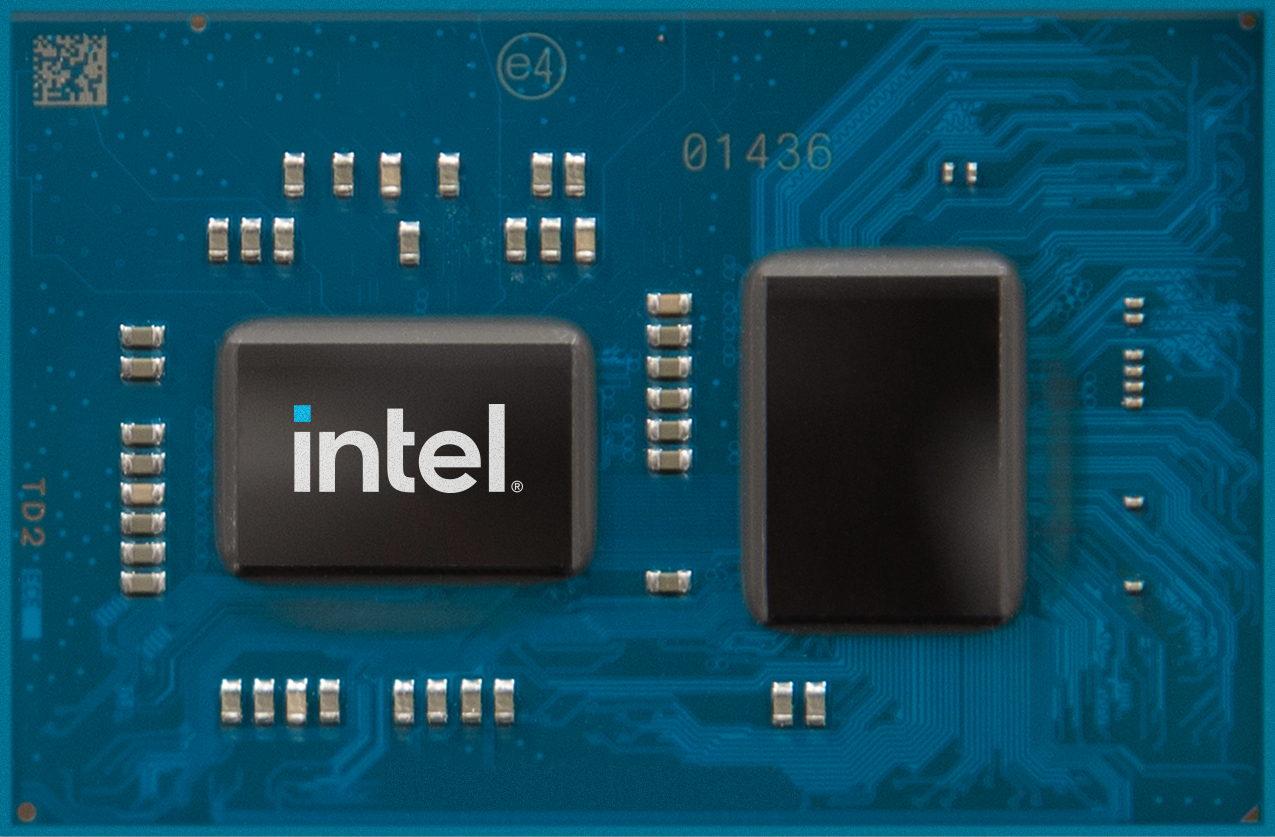
For package, Intel stated that all models will be FCBGA1493 and measure 35x24mm. Interestingly enough, this means we can calculate estimates for the die size.
- CPU die (left): 9.169 mm * 6.394 mm = 58.63 mm2
- PCH die (right): 6.369 mm * 9.778 mm = 62.27 mm2
The CPU is built on 10nm Superfin, the PCH die is built on 14nm. Note that in our recent review of the Tiger Lake UP3 processor, the PCH die for that processor with callipers was measured at 56.4 mm2. Given the rough nature of how we calculate these things, I might be inclined to believe that this mockup of Elkhart Lake might simply be the PCH die rotated and changed slightly, rather than a true-to-life example of the processor.
There's no word from Intel when these might be coming to low-power consumer products. Being built on 10SF, I suspect that the die cost might be higher than what we're normally used to. These new parts were announced as part of Intel's Industrial Summit, and as such these product managers wouldn't necessarily know what the client division would be preparing with the same silicon.
But Wait, There’s More!
Intel isn’t only announcing these new 10nm Atoms today. For the embedded applications that need more performance, there will be versions of the Tiger Lake UP3 mobile processors also for embedded markets. These are the same as the client versions of the processors, however with lower peak turbo frequencies. There will be a focus on enabling industrial workloads though the Xe graphics, AVX-512 units, and onboard neural accelerators. Real Time Computing will be enabled on the Industrial parts.
| Intel Core Embedded CPUs Tiger Lake-UP3 |
|||||||
| AnandTech | Cores | Base MHz |
Turbo MHz |
GPU EUs |
ECC | TDP | Temp ºC |
| General Embedded | |||||||
| i7-1185G7E | 4C/8T | 1200 | 4400 | 96 | No | 12-28W | 0-100 |
| i5-1145G7E | 4C/8T | 1100 | 4100 | 80 | No | 12-28W | 0-100 |
| i3-1115G4E | 2C/4T | 1700 | 3900 | 48 | No | 12-28W | 0-100 |
| Industrial Embedded | |||||||
| i7-1185GRE | 4C/8T | 1200 | 4400 | 96 | Yes | 12-28W | -40-100 |
| i5-1145GRE | 4C/8T | 1100 | 4100 | 80 | Yes | 12-28W | -40-100 |
| i3-1115GRE | 2C/4T | 1700 | 3900 | 48 | Yes | 12-28W | -40-100 |
All three are also offered with In-Band ECC and a -40ºC to 100ºC temperature window, however these have the same SKU names as the ones we've already listed. Just to confuse things.
Update: Turns out the documents we were given ahead of the launch had a number of typos in the specifications. The article has been updated.
Related Reading
- Intel's new Atom Microarchitecture: The Tremont Core in Lakefield
- Intel Lists New Atom Core: Tremont to Come After Goldmont Plus
- Intel’s Tiger Lake 11th Gen Core i7-1185G7 Review and Deep Dive: Baskin’ for the Exotic
- Intel’s 11th Gen Core Tiger Lake SoC Detailed: SuperFin, Willow Cove and Xe-LP
- The Intel Lakefield Deep Dive: Everything To Know About the First x86 Hybrid CPU


55 Comments
View All Comments
Unashamed_unoriginal_username_x86 - Wednesday, September 23, 2020 - link
How will AMDSuperFan fare against IntelSuperFan? I think IntelSuperFin has AMDSuperFan on contrarian fact denial for sure but will they be able to whine about shills and their rival company's objective inferiority like we expect r/AMD to do?kgardas - Wednesday, September 23, 2020 - link
Zephyr is not Intel's own, it's Zephyr RTOS project under Linxu Foundation umbrella. https://www.zephyrproject.org/ -- I hope Intel will submit their BSP sources there too.Ian Cutress - Wednesday, September 23, 2020 - link
Yes, I know this. What Intel is using is a Zephyr-like implementation of their own design.factual - Wednesday, September 23, 2020 - link
Zephyr is sort of Intel's own. The project started at Intel when they open sourced Rocket RTOS back when they Wind River was part of Intel.kgardas - Wednesday, September 23, 2020 - link
Those iX-11x5GxE with AVX-512, Xe and ECC RAM support looks interesting. So far only ECC + AVX-512 were Xeon and they were not available on small boards with GPIO.yeeeeman - Wednesday, September 23, 2020 - link
So the only 4.5W TDP product is a 2 core Atom at 1Ghz? Wtf?Jorgp2 - Wednesday, September 23, 2020 - link
They cancelled their 2W atoms, 4.5w is a bit too low for them to hit.flgt - Wednesday, September 23, 2020 - link
Once you start to get to low single digit watt's you really need to start looking at supported I/O of the SoC as well. It's not necessarily all the core's fault. At some point some of the high speed I/O has to come off the table to go lower.Jorgp2 - Wednesday, September 23, 2020 - link
Yeah, the drop from a 15w TDP to 4.5w is huge. 4.5w to 2w is just as big.People don't realize that a 15w TDP design can handle a 30w turbo just fine for a few seconds, or the fact that the uncore and IO take up a watt or two at 15w TDP.
That's a quarter of your power budget at 4.5w. Cherry trail has a single PCI-E lane at 2W SDP, at 4w it's 4 lanes.
PeachNCream - Wednesday, September 23, 2020 - link
Now those Pentium and Celeron-based Elkhart Lake processors are awesome looking!!! 32EU GPUs and significant per clock performance gains should make for some exciting passively cooled laptops in the 11.6 inch range. I cannot wait to see these land in the retail space in order to pump up the compute power for 6.5W TDP fanless notebooks!