The 2020 Mac Mini Unleashed: Putting Apple Silicon M1 To The Test
by Andrei Frumusanu on November 17, 2020 9:00 AM EST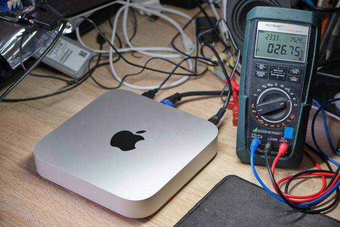
Last week, Apple made industry news by announcing new Mac products based upon the company’s new Apple Silicon M1 SoC chip, marking the first move of a planned 2-year roadmap to transition over from Intel-based x86 CPUs to the company’s own in-house designed microprocessors running on the Arm instruction set.
During the launch we had prepared an extensive article based on the company’s already related Apple A14 chip, found in the new generation iPhone 12 phones. This includes a rather extensive microarchitectural deep-dive into Apple’s new Firestorm cores which power both the A14 as well as the new Apple Silicon M1, I would recommend a read if you haven’t had the opportunity yet:
Since a few days, we’ve been able to get our hands on one of the first Apple Silicon M1 devices: the new Mac mini 2020 edition. While in our analysis article last week we had based our numbers on the A14, this time around we’ve measured the real performance on the actual new higher-power design. We haven’t had much time, but we’ll be bringing you the key datapoints relevant to the new Apple Silicon M1.
Apple Silicon M1: Firestorm cores at 3.2GHz & ~20-24W TDP?
During the launch event, one thing that was in Apple fashion typically missing from the presentation were actual details on the clock frequencies of the design, as well as its TDP which it can sustain at maximum performance.
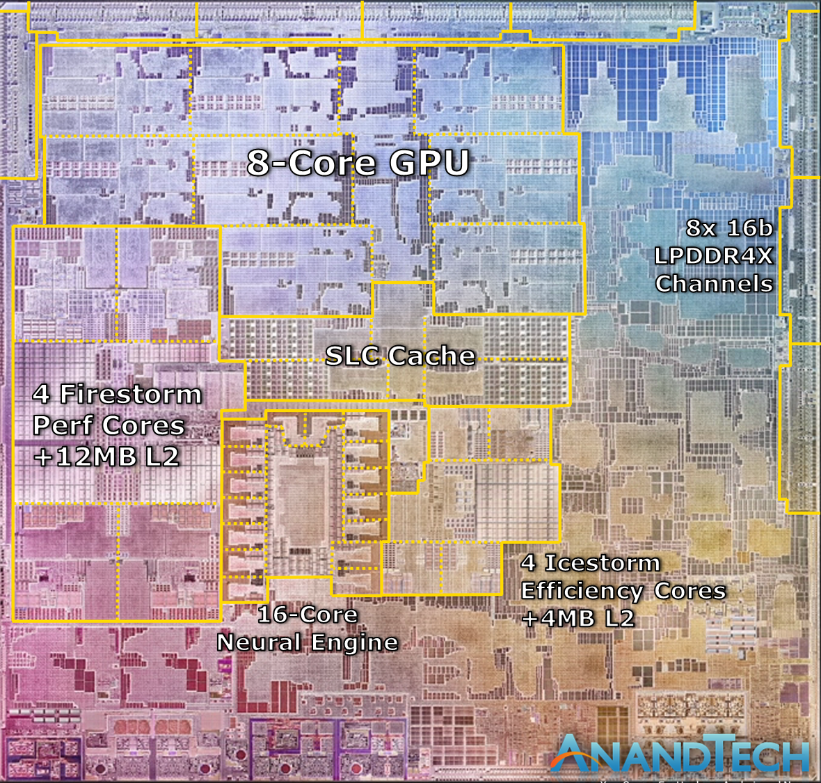
We can confirm that in single-threaded workloads, Apple’s Firestorm cores now clock in at 3.2GHz, a 6.66% increase over the 3GHz frequency of the Apple A14. As long as there's thermal headroom, this clock also applies to all-core loads, with in addition to 4x 3.2GHz performance cores also seeing 4x Thunder efficiency cores at 2064MHz, also quite a lot higher than 1823MHz on the A14.
Alongside the four performance Firestorm cores, the M1 also includes four Icestorm cores which are aimed for low idle power and increased power efficiency for battery-powered operation. Both the 4 performance cores and 4 efficiency cores can be active in tandem, meaning that this is an 8-core SoC, although performance throughput across all the cores isn’t identical.
The biggest question during the announcement event was the power consumption of these designs. Apple had presented several charts including performance and power axes, however we lacked comparison data as to come to any proper conclusion.
As we had access to the Mac mini rather than a Macbook, it meant that power measurement was rather simple on the device as we can just hook up a meter to the AC input of the device. It’s to be noted with a huge disclaimer that because we are measuring AC wall power here, the power figures aren’t directly comparable to that of battery-powered devices, as the Mac mini’s power supply will incur a efficiency loss greater than that of other mobile SoCs, as well as TDP figures contemporary vendors such as Intel or AMD publish.
It’s especially important to keep in mind that the figure of what we usually recall as TDP in processors is actually only a subset of the figures presented here, as beyond just the SoC we’re also measuring DRAM and voltage regulation overhead, something which is not included in TDP figures nor your typical package power readout on a laptop.
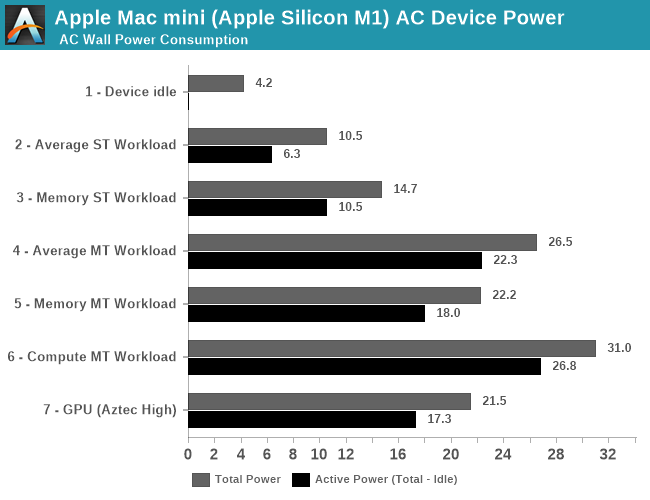
Starting off with an idle Mac mini in its default state while sitting idle when powered on, while connected via HDMI to a 2560p144 monitor, Wi-Fi 6 and a mouse and keyboard, we’re seeing total device power at 4.2W. Given that we’re measuring AC power into the device which can be quite inefficient at low loads, this makes quite a lot of sense and represents an excellent figure.
This idle figure also serves as a baseline for following measurements where we calculate “active power”, meaning our usual methodology of taking total power measured and subtracting the idle power.
During average single-threaded workloads on the 3.2GHz Firestorm cores, such as GCC code compilation, we’re seeing device power go up to 10.5W with active power at around 6.3W. The active power figure is very much in line with what we would expect from a higher-clocked Firestorm core, and is extremely promising for Apple and the M1.
In workloads which are more DRAM heavy and thus incur a larger power penalty on the LPDDR4X-class 128-bit 16GB of DRAM on the Mac mini, we’re seeing active power go up to 10.5W. Already with these figures the new M1 is might impressive and showcases less than a third of the power of a high-end Intel mobile CPU.
In multi-threaded scenarios, power highly depends on the workload. In memory-heavy workloads where the CPU utilisation isn’t as high, we’re seeing 18W active power, going up to around 22W in average workloads, and peaking around 27W in compute heavy workloads. These figures are generally what you’d like to compare to “TDPs” of other platforms, although again to get an apples-to-apples comparison you’d need to further subtract some of the overhead as measured on the Mac mini here – my best guess would be a 20 to 24W range.
Finally, on the part of the GPU, we’re seeing a lower power consumption figure of 17.3W in GFXBench Aztec High. This would contain a larger amount of DRAM power, so the power consumption of Apple’s GPU is definitely extremely low-power, and far less than the peak power that the CPUs can draw.
Memory Differences
Besides the additional cores on the part of the CPUs and GPU, one main performance factor of the M1 that differs from the A14 is the fact that’s it’s running on a 128-bit memory bus rather than the mobile 64-bit bus. Across 8x 16-bit memory channels and at LPDDR4X-4266-class memory, this means the M1 hits a peak of 68.25GB/s memory bandwidth.
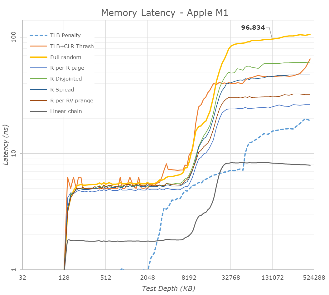
In terms of memory latency, we’re seeing a (rather expected) reduction compared to the A14, measuring 96ns at 128MB full random test depth, compared to 102ns on the A14.
Of further note is the 12MB L2 cache of the performance cores, although here it seems that Apple continues to do some partitioning as to how much as single core can use as we’re still seeing some latency uptick after 8MB.
The M1 also contains a large SLC cache which should be accessible by all IP blocks on the chip. We’re not exactly certain, but the test results do behave a lot like on the A14 and thus we assume this is a similar 16MB chunk of cache on the SoC, as some access patterns extend beyond that of the A14, which makes sense given the larger L2.
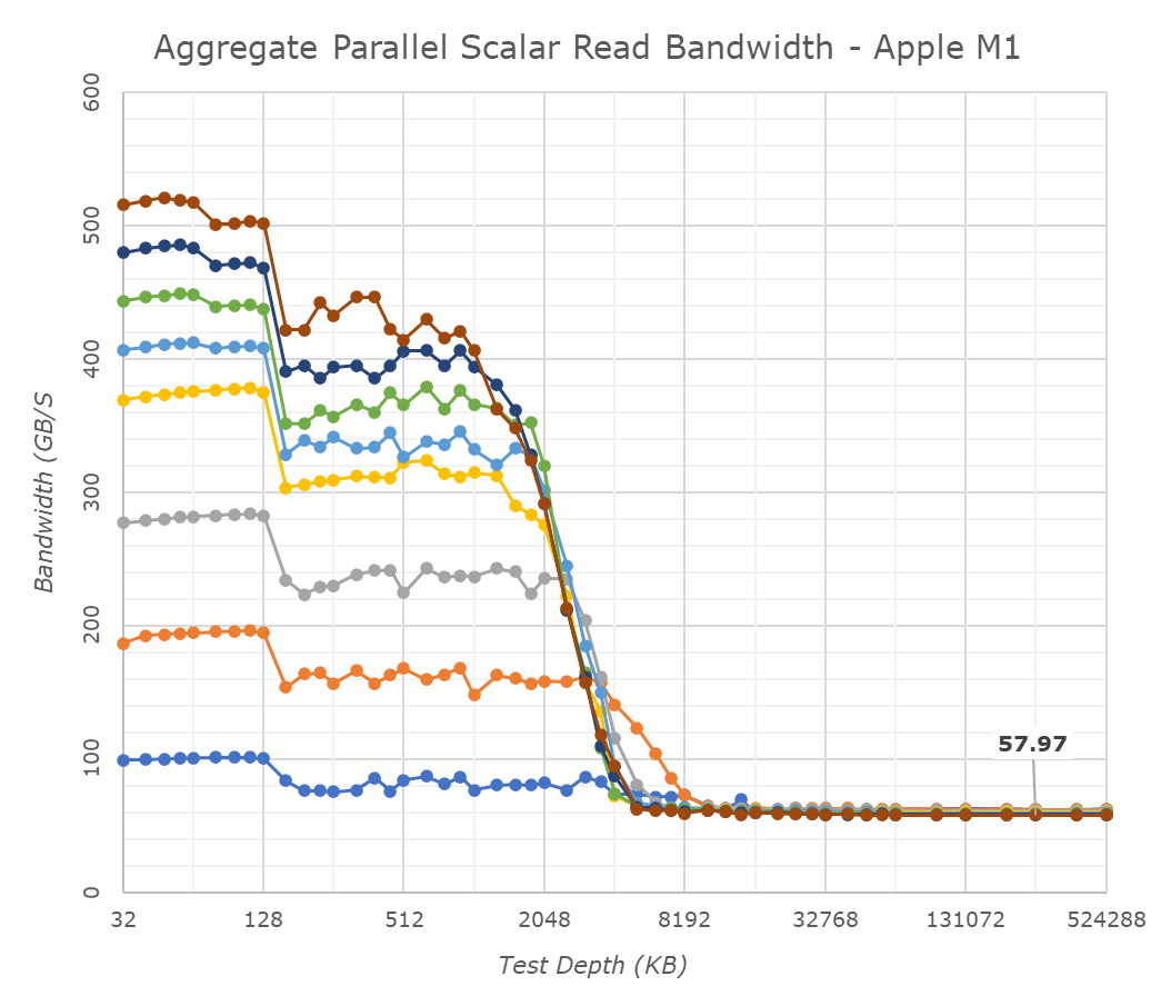
One aspect we’ve never really had the opportunity to test is exactly how good Apple’s cores are in terms of memory bandwidth. Inside of the M1, the results are ground-breaking: A single Firestorm achieves memory reads up to around 58GB/s, with memory writes coming in at 33-36GB/s. Most importantly, memory copies land in at 60 to 62GB/s depending if you’re using scalar or vector instructions. The fact that a single Firestorm core can almost saturate the memory controllers is astounding and something we’ve never seen in a design before.
Because one core is able to make use of almost the whole memory bandwidth, having multiple cores access things at the same time don’t actually increase the system bandwidth, but actually due to congestion lower the effective achieved aggregate bandwidth. Nevertheless, this 59GB/s peak bandwidth of one core is essentially also the speed at which memory copies happen, no matter the amount of active cores in the system, again, a great feat for Apple.
Beyond the clock speed increase, L2 increase, this memory boost is also very likely to help the M1 differentiate its performance beyond that of the A14, and offer up though competition against the x86 incumbents.
- Page 1: Apple Silicon M1: Recap, Power Consumption
- Page 2: Benchmarks: Whatever Is Available
- Page 3: M1 GPU Performance: Integrated King, Discrete Rival
- Page 4: SPEC2006 & 2017: Industry Standard - ST Performance
- Page 5: SPEC2017 - Multi-Core Performance
- Page 6: Rosetta2: x86-64 Translation Performance
- Page 7: Conclusion & First Impressions


682 Comments
View All Comments
RedGreenBlue - Tuesday, November 17, 2020 - link
Obviously their new designs are way off the beaten path in their improvements than the canned designs by now.dotjaz - Wednesday, November 18, 2020 - link
You must be smoking something really good. A7 was a 6-wide design while CA57 was only 3-wide. Cyclone also has 4/2/2/3 (Int/Branch/LS/NEON) units while A57 only had (2+1)/1/2/2. That's completerly different design.RedGreenBlue - Wednesday, November 18, 2020 - link
I was thinking of the A6 that was the first modification of ARM’s architecture and before that they were fundamentally copies. It’s not easy to remember which article of Anand Shimpi’s commentary I read 7 or 8 years ago. https://www.anandtech.com/show/6330/the-iphone-5-r...danbob999 - Thursday, November 19, 2020 - link
They are dumb if they pay for designs which they do not use. The instruction set must be cheaper, otherwise ARM got it the wrong way.It's like saying that the cost of food at a groceries store is higher than the complete meal at the restaurant.
michael2k - Thursday, November 19, 2020 - link
It's actually more accurate to say, "Paying for the time of the restaurant's menu designer costs more than either the groceries or the meal"With an architectural license, they get access to to a specification, which is closer to a menu, recipes, and a shopping list, than a meal or groceries.
dotjaz - Wednesday, November 18, 2020 - link
No helios24 is INCORRECT. It's the top of the licensing for sure, but it also doesn't include any hard IP. It's the broadest in use case as you can do ANYTHING with it as long as you are ISA compliant. But it's also the narrowest in terms of ARM IP portfolio. For example Huwwei still hold ARM architectural license and can design their own ARM cores, but they don't have access to anything newer than CA77 because that's a different license.Architectual license is also the cheapest *once you have certain volume*. The initial licensing fee is high, BUT you don't pay much royalty on a per-core basis becase you don't use ARM IP other than ISA.
dotjaz - Wednesday, November 18, 2020 - link
Maybe this will help you understand more. The top of the pyrimid actually don't have access to ARM's standard IP portfolio at all.https://semiaccurate.com/2013/08/07/a-long-look-at...
michael2k - Thursday, November 19, 2020 - link
The article here contradicts you: https://semiaccurate.com/2013/08/07/a-long-look-at...On top of the pyramid is both the highest cost and lowest licensee count option, but those two factors are probably not directly related. The reason is this one is called an architectural license and you don’t actually get a core, you get a set of specs for a core and a compatibility test suite.
mjkpolo - Thursday, November 19, 2020 - link
Actaully nVidia purchased ARM lolHenry 3 Dogg - Friday, November 27, 2020 - link
"ARM was founded as a joint venture between Apple and Acorn."No. ARM was founded by Acorn spinning out its inhouse developed ARM chip as a separate company. Apple bought in later as an investment, and to prevent take overs that might threaten its Newton product.