Intel’s New IDM 2.0 Strategy: $20b for Two Fabs, Meteor Lake 7nm Tiles, New Foundry Services, IBM Collaboration, Return of IDF
by Dr. Ian Cutress on March 23, 2021 5:00 PM EST- Posted in
- CPUs
- Intel
- GPUs
- IBM
- 7nm
- Fab 42
- Chiplets
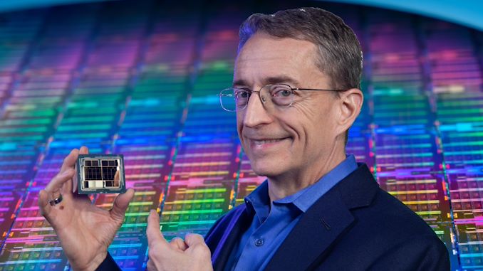
- Pat Gelsinger
- Meteor Lake
- IDF 2021
The new CEO of Intel, Pat Gelsinger, has today outlined his vision for Intel over the coming years. During an online presentation entitled ‘Intel Unleashed: Engineering The Future’, Pat Gelsinger outlined five key topics upon which Intel will work towards and what it means for the company at large. At the center of this is a reaffirmed commitment for Intel to retain its own fabs, but also double down on its ability to drive the latest technologies at scale by building new manufacturing facilities inside the US.
Highlights of Intel’s Announcements Today
- Two new fabs in Arizona, $20b investment
- New Intel Foundry Services, offering Intel manufacturing to customers
- Next generation 7nm chiplets for ‘Meteor Lake’ will finish design in Q2 2021
- New research collaboration with IBM in foundational semiconductor design
- New Intel Innovation event in Oct 2021, Spirit of IDF
We're Keeping the Fabs: Please Stop Asking
Since the start of the year, previous Intel CEO Bob Swan and new Intel CEO Pat Gelsinger have both done the equivalent of shouting from the rooftops when it comes to Intel’s market advantages. At the top of that list is Intel’s vertical integration between manufacturing and chip design, enabling Intel to control the process from top to bottom more closely than any of its chip competitors. This unique proposition labels Intel as an IDM (integrated device manufacturer) or having an IDM model (integrated device manufacturing model), and the only company that can even come close to Intel in this regard is Samsung. Intel’s plus over its competitor here is that it can apply its own designs to a scale that Intel is often attributed to.
In recent months there have been comments from analysts and investors about the potential for Intel to spin out its manufacturing plants and facilities into a separate business, similar to how AMD detached its manufacturing facilities into a new company called GlobalFoundries. The benefits of this move would allow Intel to segregate the losses between the two sides of the business, and showcase the core Intel product teams in a better light by comparison to the manufacturing arm. This sort of path has significant pitfalls, most importantly that Intel’s manufacturing main customer is Intel. GlobalFoundries had this problem initially, but Intel’s foundry arm is on a much larger scale.
So to that end, Pat Gelsinger today is hoping to put those rumors to rest, more than he stated on Intel’s 2020 financial call. Not only is Intel going to retain its manufacturing facilities, but it is going to embrace a new era of manufacturing, which is going to be called IDM 2.0.
IDM 2.0: Build, Expand, and Productize
This direction from Intel is built upon, first and foremost, the enthusiasm of Pat Gelsinger rejoining the company. Since even before he took over the role of CEO, former Intel engineering experts were coming out of retirement to work on exciting new products with Pat at the helm.
IDM 2.0 will have several pieces to the puzzle.
Build (7nm)
Today Intel will be announcing a $20 billion (USD) investment in two new manufacturing facilities (fabs) in Arizona, set to come online for production in 2024. Gelsinger will point out today that Intel is ready to break ground, increasing the number of factories on Intel’s Ocotillo campus (Chandler, AZ) from four to six.
These new fabs will be on leading edge process node technologies, with Intel extending cooperation with the State of Arizona, as well as the current administration’s target of improving semiconductor manufacturing inside the country. All parties involved seem raring to go, and Intel will be seeking to outfit its production facilities with the equipment necessary to enable leading edge manufacturing, including using Extreme Ultra Violet (EUV) technology.
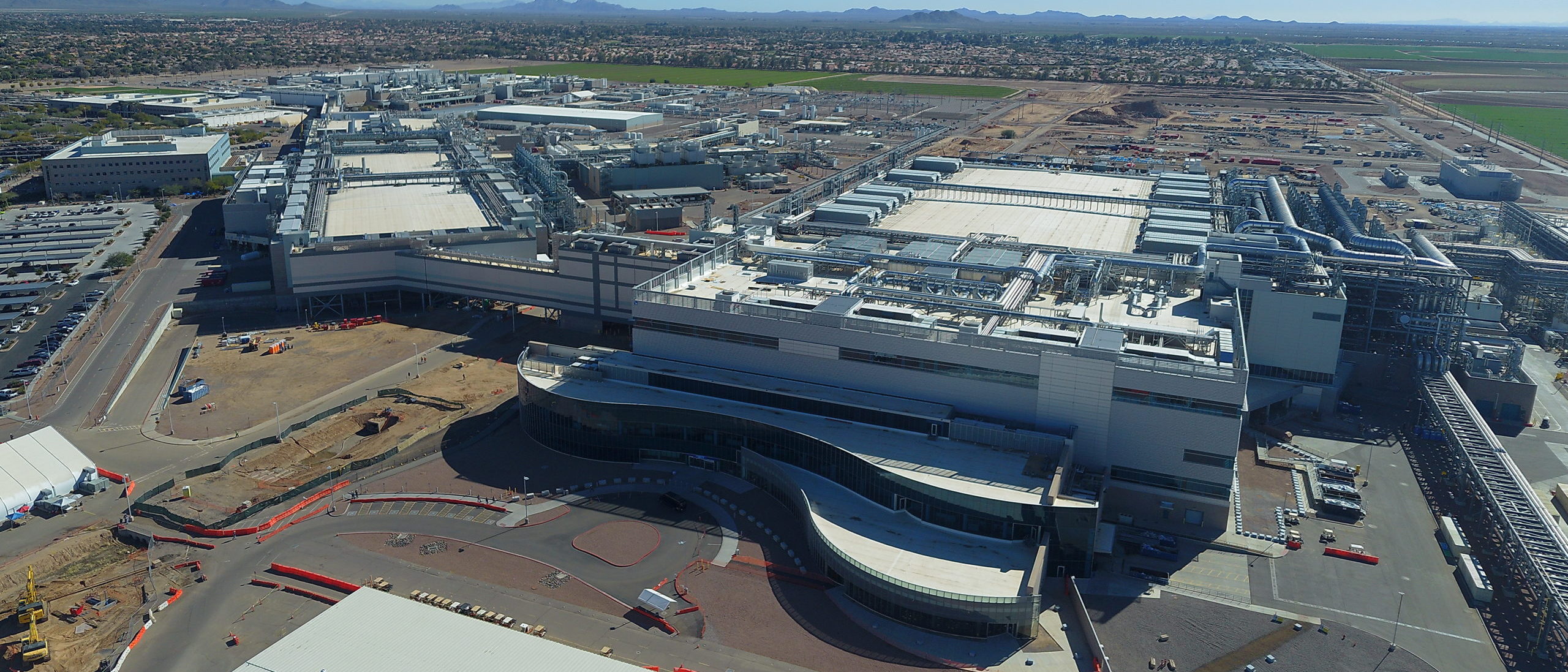
Intel's Ocotillo campus, Fab 42, Chandler AZ
It is noteworthy that the machines that enable EUV manufacturing are only supplied by a single company, ASML, and demand for these machines is at a record high, with a waiting list of over a year. Intel believes that its technology, with its increasing use of EUV to simplify manufacturing and enabling higher performance and higher yielding products, will be fully aligned and there will be enough EUV to go around by the time these new fabs are up and running.
The two new fabs are expected to bring 3000+ high wage jobs direct with Intel, 3000+ construction jobs for construction during the project, and up to 15000 long-term ecosystem support jobs for the area. Planning for construction activities are expected to start immediately. That being said, TSMC has also indicated plans to build a factory in Arizona as well, likely in the Phoenix area, with Samsung also considering a site there (or Austin, TX). There have been questions as to the sustainability of supporting that many semiconductor manufacturing plants in a single city. Intel states that it already recycles 9 million gallons (US gal.) of water each day, and the company purchases green power for its facilities, as well as on-site alternative energy projects.
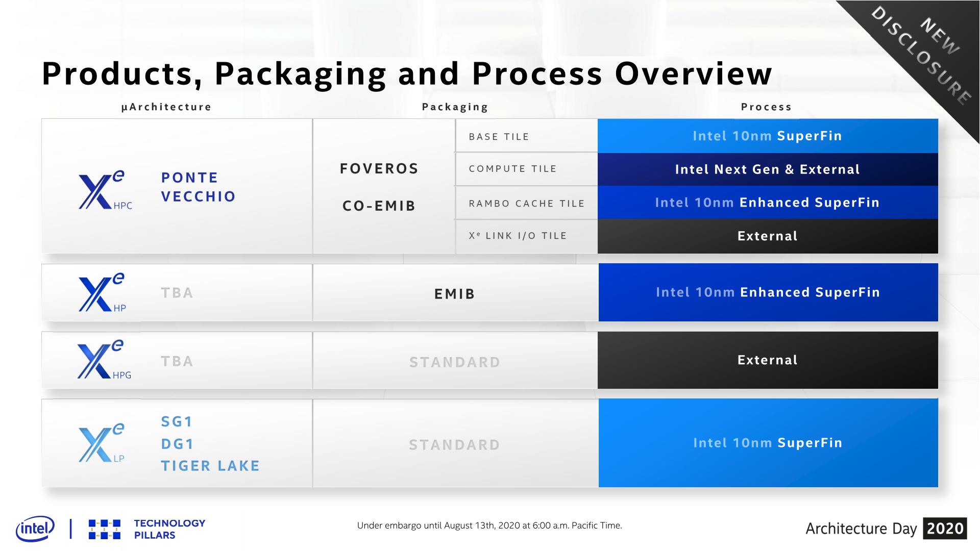
As part of this side of the announcement, Pat Gelsinger will be stating today that the 7nm manufacturing node from Intel is now running on schedule, with a solid footing. The first product enabled with 7nm will be Ponte Vecchio, the upcoming high-performance compute accelerator for the Aurora supercomputer, however end-users might be more interested in Meteor Lake, a client CPU compute tile for a volume 2023 product. Intel will announce today that the compute tile / chiplet will finish tape-in (design IP verification) by Q2 2021, and will leverage Intel’s advanced packaging techniques. After design manufacturing, tape-out (whole chip design verification) usually takes 4-6+ months, and then the designs are sent to the fabs for initial production and test runs. Given that Intel is talking about Meteor Lake as a chiplet design, starting with this compute tile, then no doubt an IO related chipset will be announced at a later time. Intel has a number of packaging technologies it could deploy here, such as EMIB or Foveros, depending on the cost intercept of the intended market.
Edit: Gelsinger confirmed that Meteor Lake will have Foveros technology.
Expand (TSMC)
Alongside building new manufacturing facilities, Intel today will reaffirm its roadmap to use a mixture of internal and external process node manufacturing depending on the product capabilities. Intel already makes heavy use of external partners, such as TSMC, and already spends enough to account for 6-7% of TSMC's annual revenue. But today’s announcement will double down on ensuring that Intel is ready to use the right process at the right time for the right products.
This includes developing its leading edge products on external foundry offerings. As Intel moves more into a chiplet ecosystem (Intel is calling it ‘tiles’), the company is prepared to manufacture its high-performance computing chiplets on external foundries. This means in both client and the datacenter, and likely means we will be seeing the latest x86 cores enabled beyond Intel. Exact announcements will follow.
Gelsinger’s presentation today will discuss that using external partners like TSMC, Samsung, GlobalFoundriers, and UMC, will allow the company to optimize roadmaps for cost, performance, schedule, and supply. This does somewhat go against the grain of the IDM 2.0 messaging, where Intel can control its own supply chain and expand production as required, however Intel expects it can find a happy medium.
Productize (IFS)
The two new manufacturing plants / fabs also filter under this Expand section, however this area is more focused on how Intel will keep those fabs fully occupied. Other semiconductor manufacturers in the market, such as TSMC, Samsung, GlobalFoundries, SMIC etc, they all have what are called foundry services which allow customers to build silicon using their manufacturing technology. With today’s announcement, the company is ready to enable its external Intel Foundry Services (IFS) to new customers. IFS will be a standalone company, with unique access to Intel's current and future offerings.
Intel has made silicon for others before, so this isn’t new. However, that project came at a time where Intel’s 10nm faltered, and the company lost a number of high-profile contracts with partners as a result. One of the issues is that Intel at the time used so many customized software tools in its silicon design process that it limited its customers’ access to these tools to build processors. This made the whole process very complicated.
The new Intel Foundry Services look will be a lot different. Intel today will have partnership announcements with Cadence and Synopsys to enable industry standard design tools (EDA tools) and workflows such that customers can use industry standard process development kits (PDKs) to build their silicon designs. This is part of the job that some of Intel’s hires have recently been enabling, such as Renduchintala, Keller, and Koduri. Intel is committing to embracing the entire EDA ecosystem to ease new customers into the use of Intel’s foundry tools.
There will be somewhat of a black cloud over Intel on how its external foundry offerings have failed in the past, however Gelsinger and the company are hoping that commitments to industry standards will help on that path to rebuilding trust and reputation.
As part of Intel’s Foundry Services, the company is announcing that it will work with customers to build SoCs with x86, Arm, and RISC-V cores, as well as leveraging Intel’s IP portfolio of core design and packaging technologies. What will be key here is the extent of exactly how Intel will offer its x86 designs – it could offer them in a licensing style similar to Arm, allowing customers to go build their own SoCs, or it could be only in a custom design services model, where you tell Intel what you want and they design/manufacture it for you. More details about how this will work is expected to come through the year.
The drive into Foundry Services is an obvious choice for Intel. Demand for semiconductor manufacturing is at an all-time high, and discussions about keeping manufacturing inside the US has been a key talking point for over a year. Intel has stated that it has keen enthusiastic support from the industry for IFS, but it will also disclose later in the year how it will expand its manufacturing capabilities in other parts of the world, such as Europe.
Collaboration with IBM, New Intel Events for Engineers
Alongside the core IDM 2.0 path, Intel also has announcements relating to the future of its R&D roadmap, as well as its outreach to engineers and commercial partners.
The collaboration with IBM on process node development and development of next-generation logic is the wildcard of today’s announcements. The two companies are set to work together on foundational technologies to move the needle on both semiconductor performance and semiconductor efficiency. The collaboration will scale through to the ecosystem, with a significant nod towards key US government initiatives.
Intel’s announcement today on this is light on details. The teams from both Oregon and New York would seem to initially start separate with collaboration-at-a-distance, although the nature of the wording of the announcement would seem to suggest that the two will come together with a semi-unified team at a later date. Intel is keeping details on the topics for research at a very high-level, but both companies have a range of expertise on fundamental silicon design as well as complex manufacturing. This might also be a nod to IBM getting access to Intel’s leading edge technologies for its POWER and z product offerings.
Also on the cards is Intel’s new series of events for engineers and commercial partners. Broadly marketed as Intel’s *on series, Gelsinger aims to rekindle the spirit behind Intel’s previous popular events such as Intel’s Developer Forum (IDF) with a new range of Intel Vision (commercial) and Intel Innovation (engineering) outreach.
The first of these events will be an Intel Innovation Event, coming in October later this year in San Francisco. If we are travelling to events again, no doubt we will be there to report on the highlights of Intel’s strategy at that point of time.
Pat Gelsinger’s Intel Legacy: Part One
Over the many interviews that Gelsinger has given over the years, his love of Intel is a persistent thread. Having finished his degree at the early age of 18, he was hired straight out of college and spent over 30 years at the company, reaching the title of Chief Technology Officer. Gelsinger then spent 12 years at EMC (now Dell EMC) and VMWare, and has come back as CEO. The hiring of an engineer at the top of the company has, in Intel’s own words, reinvigorated the enthusiasm of its engineering base.
It’s no secret that while Intel has been rewarded with record revenues these past five years, the state of play of Intel’s manufacturing roadmaps have stalled. Intel’s future has been in flux, affecting employees and followers of the company alike, leading to many column inches about how the company moves forward. The announcement of Pat Gelsinger to the role of CEO, plus his remarks during Intel’s FY2020 call, seems to have lit a fire inside Intel. Today’s announcements are the first stage in Pat Gelsinger building his CEO legacy at the company.
Intel’s path with the announcements today is very much towards a more flexible Intel. In the past where the company was rigid with its designs, rigid with its manufacturing, it is clear that Gelsinger wants to be more open and accepting of industry standard manufacturing whilst at the same time re-offering its facilities to external customers. The mantra of Intel staying on Intel manufacturing also seems to dissolve slightly, with Gelsinger not afraid to mention the name of other foundry offerings that Intel is prepared to use.
Our discussions with employees at Intel who know Pat Gelsinger have repeatedly said that he likes to ‘geek out’ over the details of new technology, and will happily sit for hours talking about both the direction of the industry as well as how Intel is positioned alongside its competition. Pat, if you’re reading this, we’re ready to geek out whenever you are.


159 Comments
View All Comments
Bagheera - Thursday, March 25, 2021 - link
this is a good readhttps://semiwiki.com/semiconductor-manufacturers/i...
GeoffreyA - Thursday, March 25, 2021 - link
Thanks! I will read it.Oxford Guy - Wednesday, March 24, 2021 - link
I guess the pretense of journalistic neutrality has gone out the window.‘to work on exciting new projects”
“raring to go”
Superheroes and supermonopolies (ASML) make me rather queasy.
GeoffreyA - Thursday, March 25, 2021 - link
"raring to go"As a Baldur's Gate fan, this reminds me of Minsc's phrase, something something and raring to go. Minsc and Boo certainly had the best lines.
eva02langley - Wednesday, March 24, 2021 - link
Intel will lose against TSMC. They will never beat their nodes. TSMC will be on 3nm in 2023... and let me remind you that 7nm is garbage. Bob Swan said the following...https://www.tomshardware.com/news/intel-announces-...
For perspective, rival foundry TSMC plans to be on the 3nm node in the same time frame as Intel's new schedule for 7nm. Intel clearly isn't pleased with its execution on the 7nm node, as an embattled Swan remarked that "And we feel pretty good about where we are, though we’re not happy. I’m not pleased with our 7nm process performance" at the end of the call after a bruising question and answer session with analysts. Swan also said "we have root-caused the [7nm] issue and believe there are no fundamental roadblocks," and that the company would provide further updates at an upcoming Architecture Day.
JayNor - Wednesday, March 24, 2021 - link
that quote was from July 2020. They did six months of experiments and Bob Swan declared the problem resolved in the q4 earnings call.eva02langley - Friday, March 26, 2021 - link
Like 10nm is resolved? No but seriously, are you for real? You are doing Intel's Damage Control? I hope you are paid for that. /sarcasmWaltC - Wednesday, March 24, 2021 - link
Same old Intel...what the company needs very, very badly are new architecture x86 CPUs, but of course Intel is throwing tons of money out to see what happens--to see what the proverbial, distant, 7nm cat drags in. Intel's idea of progress is doubling, tripling its immediate overhead with seemingly no recognition of the fact that by the time Intel brings its FABs to parity with where TSMC is right now, 7nm, TSMC will be heavily into 5nm if not 3nm, and Intel will still be far behind. Typical Intel--does not know how to do much more than throw good money after bad (Gelsinger remembers Itanium well, I'm sure) and to make stupid assumptions about its invulnerability and longevity. AMD would simply not exist today if it was crippled by the same fiscal imperatives that drive Intel. AMD cannot afford to make the mistakes Intel has made and continues to make--which is probably exactly why Intel has dropped behind AMD to the massive extent that it has today. Bringing old dudes out of retirement to relive Intel's halcyon years is about as desperate as it gets, imo.WaltC - Wednesday, March 24, 2021 - link
Well, I do have something positive to say about Gelsinger, unlike Biden, I don't think he's senile...;)Hifihedgehog - Wednesday, March 24, 2021 - link
He's also a very honorable person unlike 99% of the scummy folks I have seen running these companies. He is the last person that would be having an extramarital affair. He also is a donor to many humanitarian agencies, not a corrupt money-laundering, self-serving foundation like you see Bill Gates and others in Silicon Valley using (e.g. Gates donates and invests tax-free money to the Gates Foundation, who, in turn, purchases Microsoft products and services to use to provide "free" charitable services to impoverished nations).