Arm Announces Neoverse V1, N2 Platforms & CPUs, CMN-700 Mesh: More Performance, More Cores, More Flexibility
by Andrei Frumusanu on April 27, 2021 9:00 AM EST- Posted in
- CPUs
- Arm
- Servers
- Infrastructure
- Neoverse N1
- Neoverse V1
- Neoverse N2
- CMN-700
2020 has been an extremely successful year for Arm’s infrastructure and enterprise endeavours, as it was the year where we’ve seen fruition of the company’s “Neoverse” line of CPU microarchitectures hit the market in the form of Amazon’s new Graviton2 design as well as Ampere’s Altra server processor. Arm had first introduced the Neoverse N1 back in early 2019 and if you weren’t convinced of the Arm server promise with the Graviton2, the more powerful and super-sized Altra certainly should have turned some heads.
Inarguably the first generation of Arm servers that are truly competitive at the top end of performance, Arm is now finally achieving a goal the company has had in their sights for several years now, gaining real market share against the x86 incumbents.
Fast-forward to 2021, the Neoverse N1 design today employed in designs such as the Ampere Altra is still competitive, or beating the newest generation AMD or Intel designs – a situation that which a few years ago seemed farfetched. We recommend catching up on these important review pieces over the last 2 years to get an accurate picture of today’s market:
- Arm Announces Neoverse N1 & E1 Platforms & CPUs: Enabling A Huge Jump In Infrastructure Performance
- Amazon's Arm-based Graviton2 Against AMD and Intel: Comparing Cloud Compute
- The Ampere Altra Review: 2x 80 Cores Arm Server Performance Monster
- AMD 3rd Gen EPYC Milan Review: A Peak vs Per Core Performance Balance
- Intel 3rd Gen Xeon Scalable (Ice Lake SP) Review: Generationally Big, Competitively Small
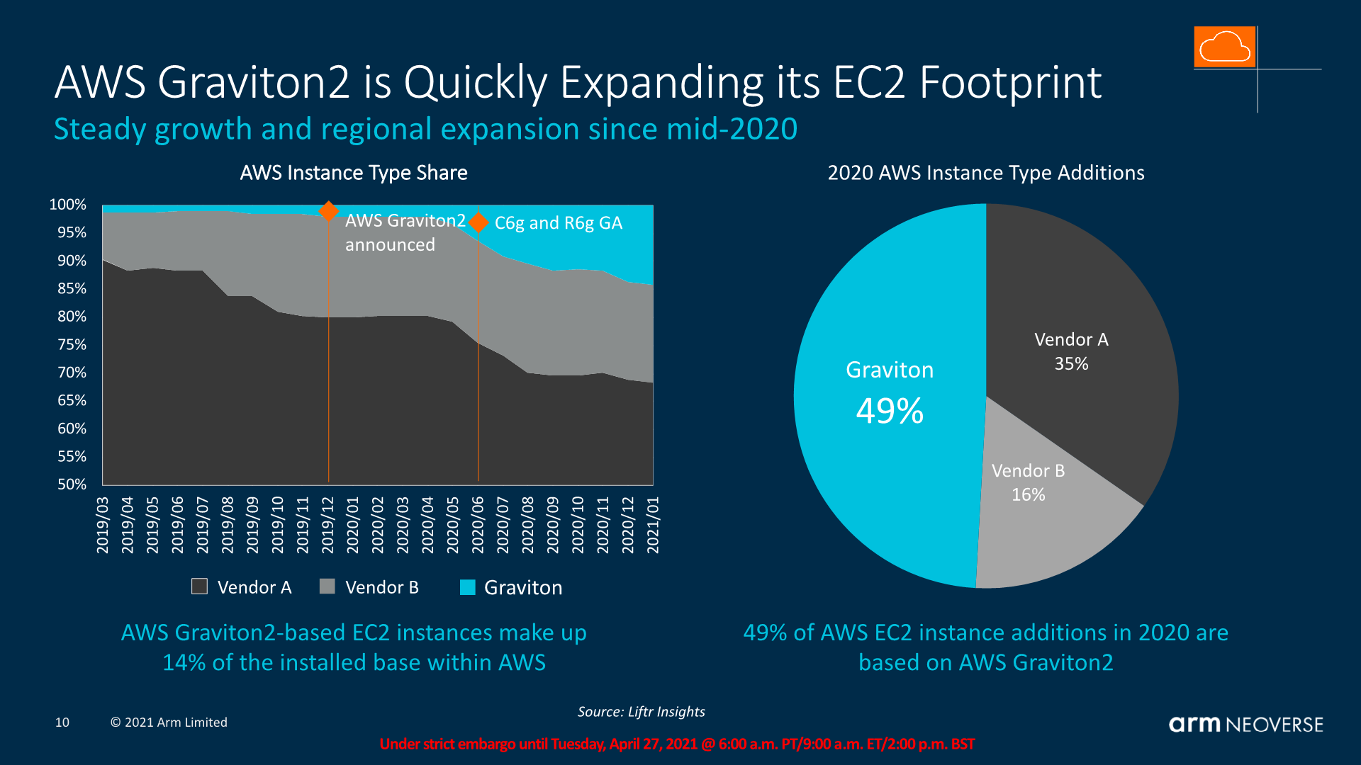
(Note: Y axis left chart starts at 50%)
Arm is very open that their main priority with the Neoverse line of products is gaining cloud footprint deployment market share, and as an example of the new-found success is an estimate into Amazon’s own AWS instance additions throughout 2020, where the new Arm-based Graviton2 is said to be the dominant hardware deployment, picking up the majority of share that’s being lost by Intel.
Looking towards 2022 and Beyond
Today, we’re pivoting towards the future and the new Neoverse V1 and Neoverse N2 generation of products. Arm had already tested the new products last September, teasing a few characteristics of the new designs, but falling short of disclosing more concrete details about the new microarchitectures. Following last month’s announcement of the Armv9 architecture, we’re now finally ready to dive into the two new CPU microarchitectures as well as the new CMN-700 mesh network.
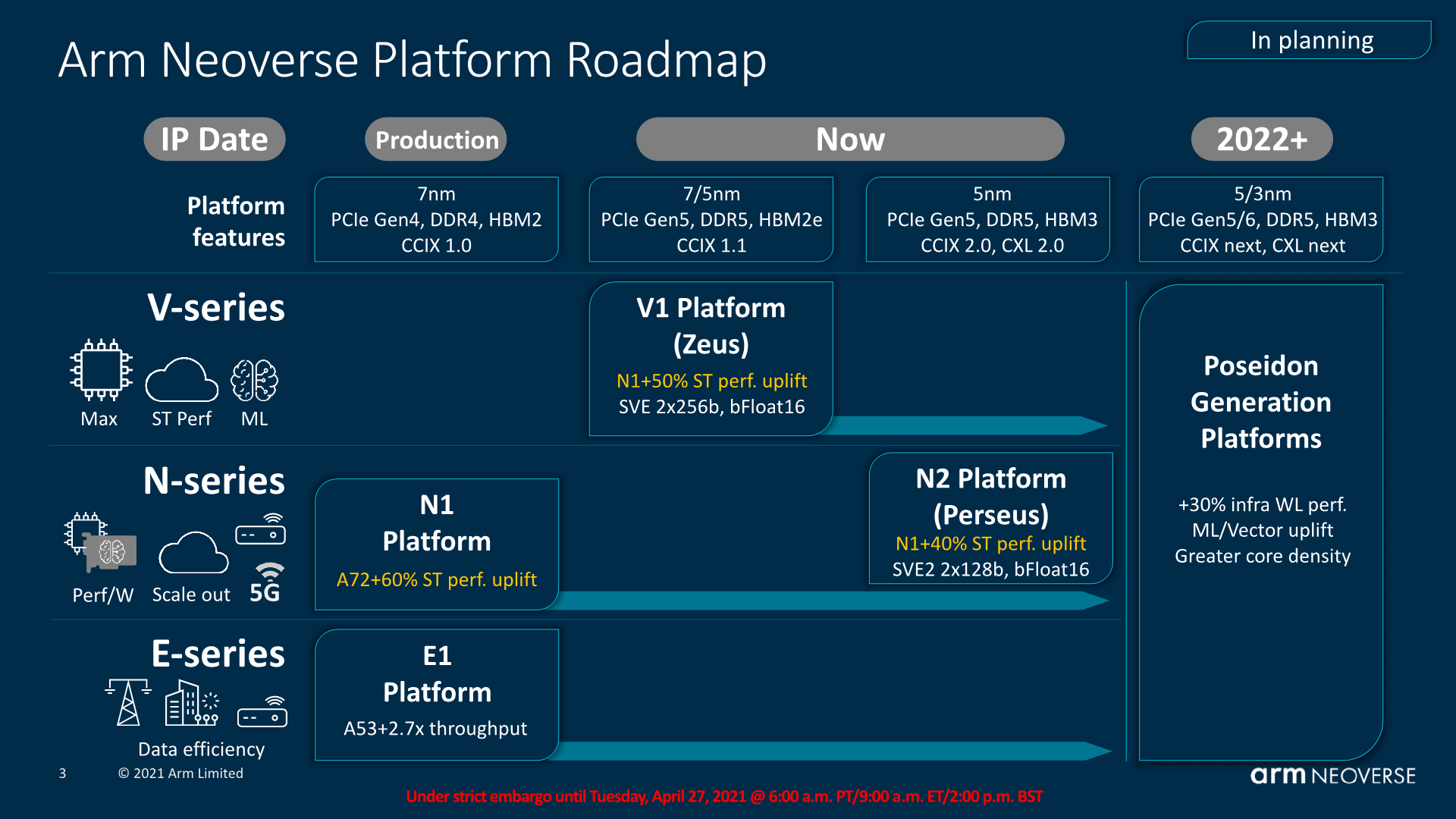
As presented back in September, this generation of Neoverse CPU microarchitectures differ themselves in that we’re talking about two quite different products, aimed at different goals and market segments. The Neoverse V1 represents a new line-up for Arm, with a CPU microarchitecture that is aiming itself for more HPC-like workloads and designs oriented towards such markets, while the Neoverse N2 is more of a straight-up successor to the Neoverse N1 and infrastructure and cloud deployments in the same way that the N1 sees itself today in products such as the Graviton or Altra processors.
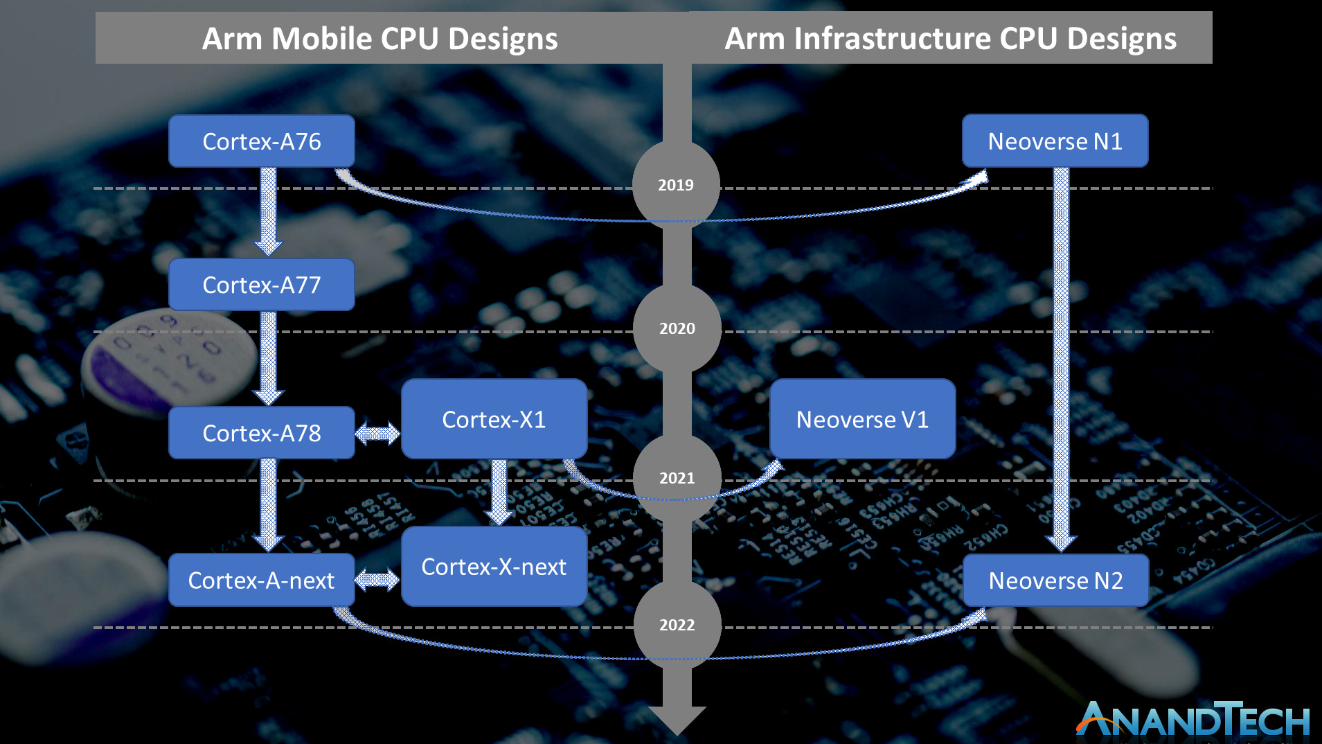
For readers who are familiar with Arm’s mobile CPU microarchitectures, there’s definitely very large similarities between the designs – even though Arm’s marketing seems to be oddly reluctant to make such kind of comparisons, which is why I made the above chart which more clearly tries to depict the similarities between design generations.
The original Neoverse N1 as seen in the Graviton2 and Altra Q processors had been a derivative, or better said, a sibling microarchitecture, to the Cortex-A76, which had been employed in the 2019 generation of Cortex-A76 mobile SoCs such as the Snapdragon 855. Naturally, the Neoverse designs had server-oriented features and changes that aren’t present in the mobile counterparts.
Similarly to how the N1 was related to the A76, the new generation V1 and N2 microarchitectures are related to newer designs in the Cortex-portfolio. The V1 is related to the Cortex-X1 which we’ve seen in this year’s new mobile SoCs such as the Snapdragon 888 or Exynos 2100. The Neoverse N2 on the other hand is related to an upcoming new Cortex-A microarchitecture which we expect to hear more about in the following few months. Throughout the piece today we’ll make a few more references to this generational disconnect between the V1 and N2, and it’s important to remember that the N2 is a newer design, albeit aimed at different performance and efficiency points.
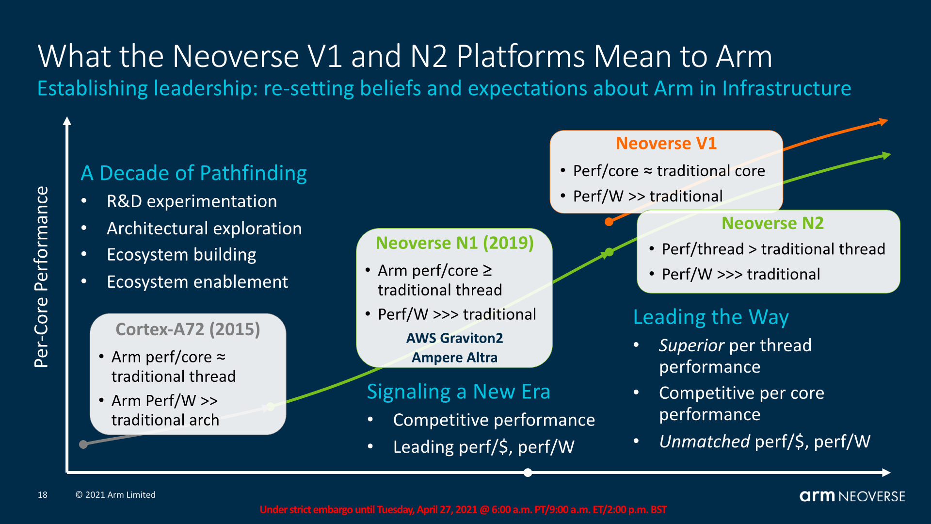
This decoupling of design goals between the V1 and N2 for Arm comes through the company’s attempt to target more specific markets where the end products might have different priorities, much like how in the mobile space the new Cortex-X series prioritises per-core performance while the Cortex-A series continues to focus on the best PPA. Similarly, the V1 focuses on maximised performance at lower efficiency, with features such as wider SIMD units (2x256b SVE), while the N2 continues the scale-out philosophy of having the best power-efficiency while still moving forward performance through generational IPC improvements.
In today’s piece, we’ll be diving into the new microarchitectural changes of the V1, N2, as well as Arm’s newest generation mesh interconnect IP, the CMN-700, which is expected to serve as the foundation of the next-generation Arm infrastructure processors.
Table of contents:
- A Successful 2020 for Arm - Looking Towards 2022
- The Neoverse V1 Microarchitecture: X1 with SVE?
- The Neoverse V1 Microarchitecture: Platform Enhancements
- The Neoverse N2 Microarchitecture: First Armv9 For Enterprise
- The SVE Factor - More Than Just Vector Size
- PPA & ISO Performance Projections
- The CMN-700 Mesh Network - Bigger, More Flexible
- Eventual Design Performance Projections
- First Thoughts & End Remarks


95 Comments
View All Comments
name99 - Thursday, April 29, 2021 - link
What do you mean by "compare?"Apple is 8-wide Decode, Map, Rename. But that doesn't include the fact that Apple does a ton of clever work in those three stages (
- simple branches handled at Decode,
- a variety of zero-cycle moves and immediate handling in Rename
- two-level scheduler, with the higher level able to accept an 8-wide feed from Rename, even though the lower-level scheduler is narrower [6 for int, 4 for FP or LS] )
Apple is *astonishingly* wide at the completion end. 16-wide register freeing and history file release, up to 56(!!!)-wide release of ROB entries.
The Apple pattern so far (insofar as pattern-detection is worth anything) has been a 1st generation of four cores (A7/8/9/10) with similar design and 6-wide, constantly iterating on details within that framework;
then a 2nd generation (A11/12/13/14) that makes explicit the big.LITTLE structure (in A10 that was mostly invisible) and based on an 8-wide (with 6 integer units) structure.
If one has to bet, the reasonable thing to bet might be something like starting with A15 we transition to 10-wide (initially with6 later with 8 integer units), and 2xSVE256. Once again lay the framework, then scale out the pieces over the subsequent three cores.
One thing that is very clear (and presumably part of Apple's success) is that they have been very willing to keep modifying how they do things; they don't just settle on a design and leave it unchanged except perhaps for some scaling up. For example the way they handle the MOV xn, xm instruction has gone through at least three very different schemes. This may seem trivial (who cares about how a singe instruction is implemented?) except that these schemes indicate a substantial reworking of the entire register file and how registers are allocated and then freed.
This is in comparison to x86 which seems to live in (probably justified) terror that any change they make, no matter how low level, will probably break something because the whole system is so complex and so interconnected that no one person holds the entire thing in their head.
They also seem to have a good system in place for hiding new functionality behind chicken bits, so that they can effectively debug new features within shipping hardware. For example there are reasons to believe that A14 might have in place most of the pieces required for physical register file amplification (avoid allocation for back-to-back register usage and grab the intermediary off the bypass bus; early release of logically overwritten registers) but these are not visible -- probably behind chicken bits so that they can be tested under all circumstances in shipping HW, and made visible for A15.
And anyone who has not looked at the details is unaware of just how impressive the underlying Apple µArch platform is. There is substantial room there on-going growth! As I continue to explore it, not only do I see how well it works today, I also see multiple directions in which it could "easily" (ie feasibly, on schedule and within budget) be improved for years to come. The only other artifact I know of that comes close in terms of quality of implementation and ability for continuing growth is the Mathematica code base -- other artifacts like other CPUs, or various OS implementations, are in a totally different (and far inferior) league.
name99 - Thursday, April 29, 2021 - link
To expand on my point, it's great that ARM are including so many good idea, but it's also astonishing the extent to which pretty much every good idea already has an Apple precedent.For example consider the MPAM discussion: "The mechanism to which this can be achieved can also include microarchitectural features such as dispatch throttling where the core slows down the dispatched instructions, smoothing out high power requirements in workloads having high execution periods, particularly important now with the new wider 2x256b SVE pipelines for example."
This sounds like (and IS) a good idea -- certainly a lot better than reducing frequency the way Intel does for AVX512.
But look at this Apple patent from 2011(!)
https://patents.google.com/patent/US9009451B2
"A system and method for reducing power consumption through issue throttling of selected problematic instructions. A power throttle unit within a processor maintains instruction issue counts for associated instruction types. The instruction types may be a subset of supported instruction types executed by an execution core within the processor. The instruction types may be chosen based on high power consumption estimates for processing instructions of these types. The power throttle unit may determine a given instruction issue count exceeds a given threshold. In response, the power throttle unit may select given instruction types to limit a respective issue rate. The power throttle unit may choose an issue rate for each one of the selected given instruction types and limit an associated issue rate to a chosen issue rate. The selection of given instruction types and associated issue rate limits is programmable."
I just keep bumping into this stuff! Arm release new cores with what seem like good ideas (and of course ARM tell us a lot more about what's new than Apple does). I do some exploring -- and find Apple patented that idea five or more years earlier!
mode_13h - Thursday, April 29, 2021 - link
> consider the MPAM discussionThe slide calls that MPMM. The article confuses it with Memory Partitioning And Monitoring.
Anyway, the N2's PDP sounds a lot more advanced.
GeoffreyA - Friday, April 30, 2021 - link
Zen 3 needn't blush when standing next to Apple. 4-wide decode might be small but that does pick up to 6, coming out of the micro-op dispatch. Then, going down, you've got 10-wide issue on the INT side, and 6-wide on FP. Admittedly, narrower register files and 8-wide retire from the (smaller) ROB, along with smaller caches. As for move elimination, even Skylake has that. Yes, everything tends to be narrower. But I think it goes to show there's nothing particularly out of this world on the Apple side.name99 - Friday, April 30, 2021 - link
I did not say that move elimination was the interesting part.I said that what was interesting is that over Apple's short CPU career they have already implemented it in three significantly different ways.
That strikes me as interesting and important -- there is no resting on the laurels, no acceptance that "we have the feature, OK to slow down". You honestly believe that Intel operates according to that same mentality?
GeoffreyA - Friday, April 30, 2021 - link
I'll admit, Apple isn't resting; and they aren't scared to break orthodoxy in advancing their designs. If the others do not wake up, they'll be left in the dust. As for Intel, complacency has put them in the well-deserved pickle they're in today. AMD deserves credit, though, for doing much these past few years; and, like Apple, aren't resting on their laurels either (arguably like they did in the K8 era).mode_13h - Friday, April 30, 2021 - link
How big are Apple's cores, though? Area is tricky, because they tend to be on a newer process node.But, my point is that maybe AMD and Intel aren't making their cores even larger and more complex, because they're targeting the server market and found that a more area-efficient way to scale performance is by adding more cores, rather than making their existing cores even more complex.
name99 - Friday, April 30, 2021 - link
A14 is 88mm^2.Eyeballing it, each large core is about 2.5% of that area, so 2.2mm^2
Throw in the L2 at about 3.5%, so 3mm^2 (shared between two cores).
Throw in the SLC (not exactly an L3, but pretend it is if you insist) at 8.8% and about 8mm^2.
I guess if you were targeting a server type design, we could probably treat it as something like
2.5+(3/4)+ (8.8/8) [making rough guesses about what sort of L2 and L3 would be optimal for a server type design] so ~4.4mm^2.
Could fit ~100 in a 440mm^2 (though you'd also want some memory controllers and IO!)
Definitely a lot larger than something like an N1 or N2 -- but of course, Apple isn't designing for the data center -- if they were, they'd probably adopt something halfway between Fire Storm and Ice Storm.
The problem is not that Intel and AMD are chasing the server market, it is that the way they are chasing it is incoherent. IF your primary goal is the server market, then WTF are you designing for super-high frequencies? The data center cores never run at those frequencies -- but being able to boast about them means your transistor density is half to a third that of Apple (or more relevant ARM/Altra/Graviton) on the same process...
Pick a goal and optimize for it! But Intel's goal seems to be to optimize for marketing that they can hit 5.x GHz (for half a second...) Not clear that designing the entire company around that goal (of zero interest to the data center, and little interest to most users) is such a great long-term strategy.
mode_13h - Saturday, May 1, 2021 - link
> IF your primary goal is the server market, then WTF are you designing for super-high frequencies?AMD actually has lagged Intel in frequency, and I think that's one of the reasons. Remember, AMD is the only one using the same exact silicon on both the mainstream desktop and in all their server products.
Intel, on the other hand, has completely separate silicon for their server dies, and we don't know all of the subtle ways they could differ from their desktop or laptop cores. We just know they tend to reuse the same basic core micro-architecture up and down their product lines (except for the really cheap/low-power stuff).
> The data center cores never run at those frequencies
A few Cascade Lake Xeons could turbo up to 4.5 GHz, which benefits certain workloads. The fastest turbo clock of an Ice Lake Xeon is 4.4 GHz
The fastest EPYC can boost up to 4.1 GHz.
In Intel & AMD's defense, a simpler core can clock higher, but runs more efficiently at lower clocks and enables higher densities. So, it seems like a pretty good strategy to me.
> Pick a goal and optimize for it!
Like ARM, Intel and AMD trying to balance power (in a server/laptop application, at least) and area. Apple is the only one who really has the luxury not to care much about area and just optimize for a single target. When Apple reuses its laptop core micro-architecture in both desktops AND servers, then we can compare them to the other guys. Until then, I think it's a case of Apples and pears.
GeoffreyA - Saturday, May 1, 2021 - link
"Until then, I think it's a case of Apples and pears."I think that's it. Well, soon process improvements will be a thing of the past, owing to quantum effects, and then we'll see who does what. The free ride is almost over.