AMD Demonstrates Stacked 3D V-Cache Technology: 192 MB at 2 TB/sec
by Dr. Ian Cutress on May 31, 2021 11:50 PM EST
The AMD team surprised us here. What seemed like a very par-for-the-course Computex keynote turned into an incredible demonstration of what AMD is testing in the lab with TSMC’s new 3D Fabric technologies. We’ve covered 3D Fabric before, but AMD is putting it to good use by stacking up its processors with additional cache, enabling super-fast bandwidth, and better gaming performance. That’s the claim at any rate, and AMD showcased its new demo processor on stage at Computex. Here’s a deeper run-down into what it actually is.
3D Chiplets: The Next Step
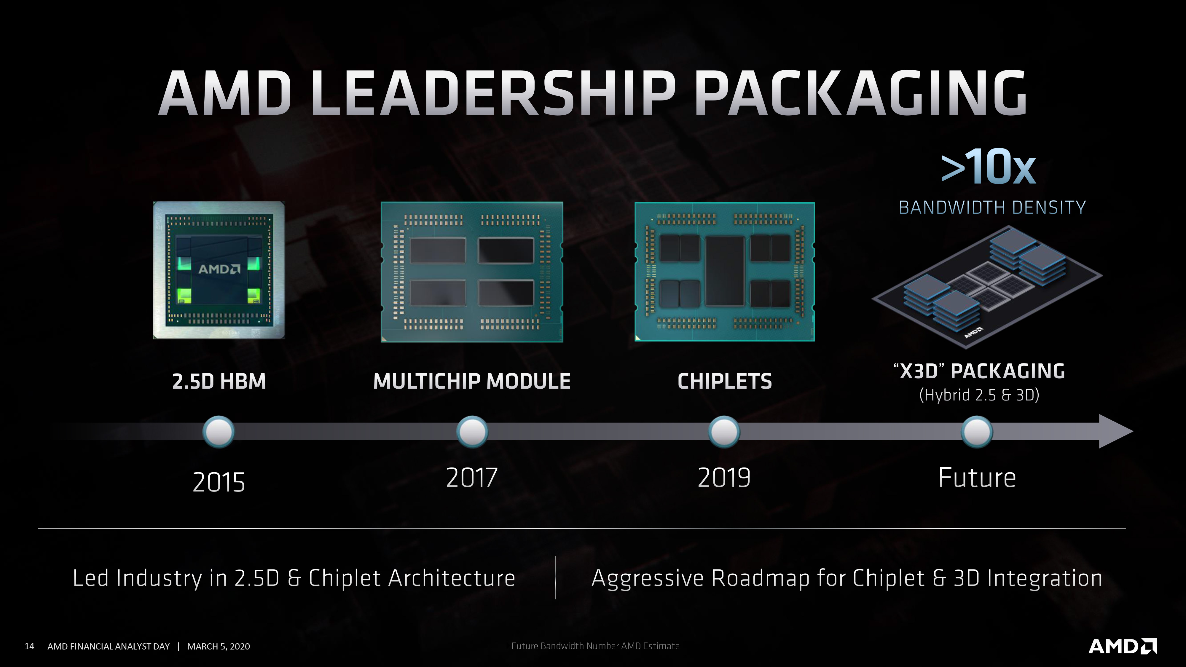
AMD announced it was looking into 3D stacking technologies with ‘X3D’ back in March 2020 at its Financial Analyst Day, with a very odd diagram showing a chiplet processor with what looked like stacks of HBM or some sort of memory around the outside. At the time AMD said it was a mix of 2.5D and 3D packaging technologies enabling 10x bandwidth density or higher. The ‘X’ in ‘X3D’ was meant to stand for Hybrid, and the technology was set for ‘the future’. Since then TSMC has announced its 3D Fabric line of technologies, a broad name for its combination of 2.5D and 3D integration offerings.
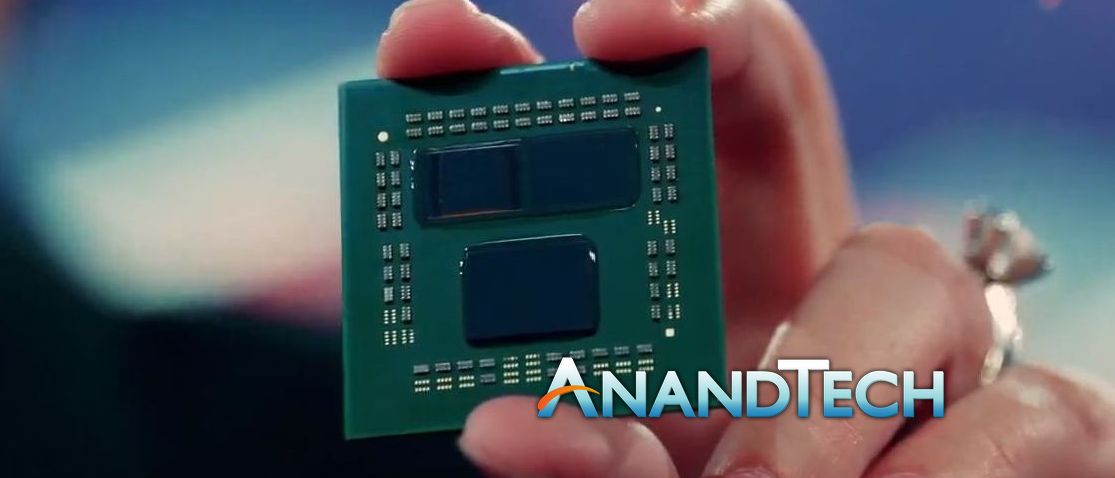
Today AMD presented the first stage of its 3D chiplet journey. The first application is a stacked cache on top of a standard processor chiplet. On stage, Lisa Su showcased one of AMD’s Ryzen 5000 dual-chiplet processors with Zen 3 cores. On one of the compute chiplets, a 64 MB SRAM built on TSMC’s 7nm was integrated on the top, effectively tripling the amount of cache that the cores have access to.
That means that the original Ryzen 5000 chiplet, with eight cores having access to 32 MB of L3 cache, now becomes an eight-core complex with access to 96 MB of L3 cache. The two dies are bonded with Through Silicon Vias (TSVs), passing power and data between the two. AMD claims that the total bandwidth of the L3 cache increases to beyond 2 TB/sec, which would technically be faster than the L1 cache on the die (but with higher latency).
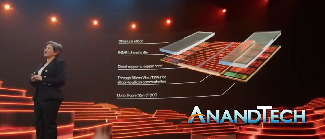
As part of the chip diagram, the TSVs would be direct copper-to-copper bonding. The cache die is not the same size as the core complex, and as a result additional structural silicon is needed to ensure that there is equal pressure across both the bottom compute die and the top cache die. Both dies are thinned, with the goal to enable the new chiplet in the same substrate and heatspreader technology currently in use in Ryzen 5000 processors.
The prototype processor shown on stage had one of its chiplets using this new caching technology. The other chiplet was left as standard to show the difference, and the one chiplet that had the cache die ‘exposed’ made it obvious and comparable with the regular non- integrated chiplet. CEO Dr. Lisa Su said that the 64 MB SRAM in this case is a 6mm x 6mm design (36 mm2), which puts it at just under half the die area of a full Zen 3 chiplet.
In a full product Lisa explained that all the chiplets would have the stacked cache enabled, for 96 MB of cache per chiplet, or 192 MB total for a processor like this that has 12 or 16 cores.
As part of the technology, it was explained that this packaging enables a >200x interconnect density compared to regular 2D packaging (which is something we already know from HBM stacking), a >15x density increase compared to microbump technology (a shot straight across the bow of Intel’s Foveros), and >3x better interconnect efficiency compared to microbumps. The TSV interface is a direct die-to-die copper interconnect, meaning that AMD is using TSMC’s Chip-on-Wafer technology. Dr Su claimed on stage that these features make this the most advanced and flexible ‘active-on-active’ chip stacking technology in the industry.
As for performance demonstrations, AMD compared a before and after using Gears of War 5. On one side was a standard Ryzen 9 5900X 12-core processor, while the other was a prototype using the new 3D V-Cache built upon a Ryzen 9 5900X. Both processors were fixed at 4 GHz, and paired with an un-named graphics card.
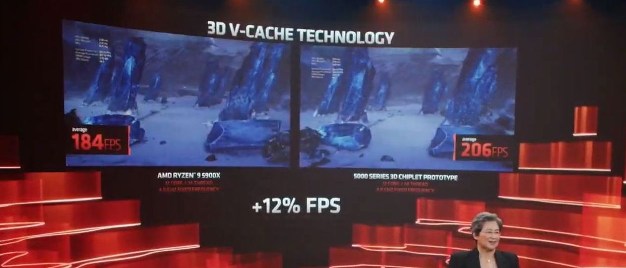
In this scenario the comparison point is that one processor has 64 MB of L3 cache, while the other has 192 MB of L3 cache. One of the selling points of Ryzen 5000 processors was the extended L3 cache available to each processor to help with gaming performance, and moving that up to 96 MB per chiplet extends that advantage even further, with AMD showing a +12% FPS gain (184 FPS vs 206 FPS) with the increased cache size at 1080p. Over a series of games, AMD claimed +15% average gaming performance:
- DOTA2 (Vulkan): +18%
- Gears 5 (DX12): +12%
- Monster Hunter World (DX11): +25%
- League of Legends (DX11): +4%
- Fortnite (DX12): +17%
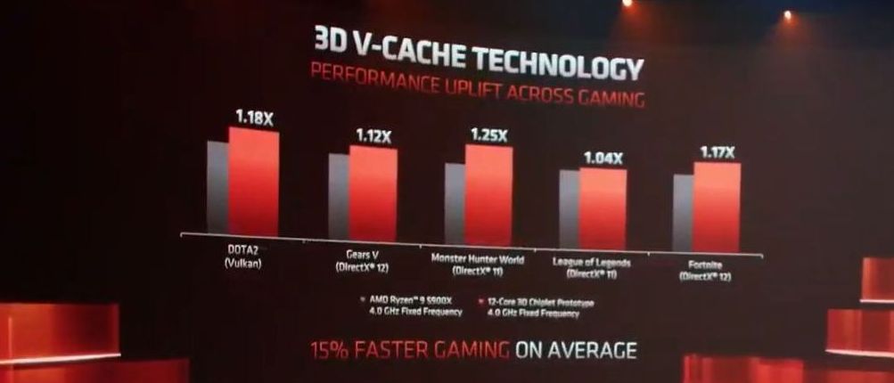
This is not an exhaustive list by any means, but it makes for interesting reading. AMD’s claim here is that a +15% bump is akin to a full architecture generation jump, effectively enabling a rare improvement through philosophical design differences. Here at AnandTech we would like to note that as it becomes harder to drill down into new process nodes, philosophical design enhancements might become the main driver of future performance.
AMD says that it has made great strides with the technology, and is set to put it into production with its highest-end processors by the end of the year. It wasn’t stated on what products it would be coming to, whether that was consumer or enterprise. Apropos of this, AMD has said that Zen 4 is set for launch in 2022.
The AnandTech Analysis
Well that was unexpected. We knew that AMD was going to be investing in TSMC’s 3D Fabric technology, but I guess we didn’t expect it to be this soon or with a demo on a desktop processor first.
Starting with the technology, this is clearly TSMC’s SoIC Chip-on-Wafer in action, albeit with only two layers. TSMC has demonstrated twelve layers, however those were non-active layers. The problem with stacking silicon is going to be in the activity, and subsequently thermals. We’ve seen with other TSV stacked hardware, like HBM, that SRAM/memory/cache is the perfect vehicle for this as it doesn’t add that much to the thermal requirements of the processor. The downside is that the cache you stack on top is little more than just cache.
This is where AMD and Intel’s stacking differs. By using TSVs rather than microbumps, AMD can get greater bandwidth and power efficiency out of TSVs, but also stack multiple chiplets high if needed. TSVs can carry power and data, but you still have to design around the two for cross signaling. Intel’s Foveros technology, while it is also 3D stacking, it relies on microbumps between the two chiplets. These are bigger and power-hungry, but allow Intel to put logic on both the lower die and upper die. The other element is thermals – usually you want the logic on the top die to manage the thermals better as it is close to the heatspreader/heatsink, but moving logic further away from the substrate means that power has to be transported up to the top die. Intel is hoping to mix microbumps and TSVs in upcoming technologies, and TSMC has a similar roadmap for the future for its customers.
Moving to the chiplet itself, it was claimed that the 64 MB L3 cache chiplet is 6mm x 6mm, or 36 mm2, and is built on TSMC 7nm. The fact that it is built on TSMC 7nm is going to be a critical point here – you might think that a cache chiplet might be better suited to a cheaper process node. The tradeoff in cost is power and die area (yield at such a small die size isn’t worth considering). If AMD is to make these cache chiplets on TSMC 7nm, then that means a Zen 3 with additional cache requires 80.7 mm2 for the Zen 3 chiplet as normal, then another 36 mm2 for the cache, effectively requiring 45% more silicon per processor. While we’re currently in a silicon shortage, this might have an effect on how many processors are made available for wider use. This might be why AMD said it was looking at ‘highest-end’ products first.
Now adding 64 MB of cache to a chip that already has 32 MB of L3 cache isn’t as straightforward as it seems. If AMD is directly integrating it as an adjacency to the L3 cache, then we have a dual-tiered L3 cache. Likely accessing that 64 MB requires more power, but that provides greater bandwidth. It would depend on the workload if the regular 32 MB is enough, compared to the extra 64 MB provided by the stacked die. We could see the extra 64 MB seen as an equivalent L4 cache, however the issue here is that in order for that extra 64 MB to go out to main memory, it has to pass through the main chiplet under it. That’s an additional power draw worth noting. I am very interested in seeing how the memory profile from the perspective of a core comes out with this extra chiplet, and how AMD is integrating that into the structure. AMD has stated that it is an SRAM-based design, so unfortunately it isn’t anything fancy like persistent memory, which would have been a whole different design ethos. By sticking to SRAM it means that at least it can seamlessly provide performance uplifts.
On the performance, we’ve seen L3 cache depth improve gaming performance, both for discrete and integrated gaming. However, increased L3 cache depth doesn’t do much else for performance. This was best exemplified in our review of Intel’s Broadwell processors, with 128 MB of L4 cache (~77 mm2 on Intel 22nm), wherein the extra cache only improved gaming and compression/decompression tests. It will be interesting to see how AMD markets the technology beyond gaming.
Finally, interception into the mainstream - AMD says that it is ready to start integrating the technology into its high-end portfolio with production at the end of the year. AMD has said that Zen 4 on 5nm launch is in 2022. Based on previous timescales, we have predicted that AMD’s next processor family is roughly a Feb 2022 launch. Whether that would be Zen 4 it’s unclear at this point, but also Zen 4 is on 5nm and AMD is showcasing this 3D V-Cache on 7nm. Whether AMD has plans to monetize this feature on 7nm, or whether it might combine a 5nm Zen 4 chiplet with a 7nm 64 MB cache chiplet is unclear. It wouldn’t be too difficult to combine the two, however I suspect that AMD might want to push its caching technology into more premium products than Ryzen desktop. We might see special one-off editions as the technology ramps through the stack.
To conclude, I have a number of questions I’d like to ask AMD. I’m hoping that I will get some answers, and if I do, I’ll cycle back with the details.
Update: June 1st:
In a call with AMD, we have confirmed the following:
- This technology will be productized with 7nm Zen 3-based Ryzen processors. Nothing was said about EPYC.
- Those processors will start production at the end of the year. No comment on availability, although Q1 2022 would fit into AMD's regular cadence.
- This V-Cache chiplet is 64 MB of additional L3, with no stepped penalty on latency. The V-Cache is address striped with the normal L3 and can be powered down when not in use. The V-Cache sits on the same power plane as the regular L3.
- The processor with V-Cache is the same z-height as current Zen 3 products - both the core chiplet and the V-Cache are thinned to have an equal z-height as the IOD die for seamless integration
- As the V-Cache is built over the L3 cache on the main CCX, it doesn't sit over any of the hotspots created by the cores and so thermal considerations are less of an issue. The support silicon above the cores is designed to be thermally efficient.
- The V-Cache is a single 64 MB die, and is relatively denser than the normal L3 because it uses SRAM-optimized libraries of TSMC's 7nm process, AMD knows that TSMC can do multiple stacked dies, however AMD is only talking about a 1-High stack at this time which it will bring to market.


93 Comments
View All Comments
psychobriggsy - Tuesday, June 1, 2021 - link
It is a prototype, and locking the clock does allow direct comparison. Apart from silicon shortage, it is possible that heat transfer issues at high clock speeds killed off the rumoured Warhol consumer chip design that probably used this.I suspect this will form the basis of Milan-X, where clock speeds are less critical over sheer quantity of cores and cache.
Kevin G - Tuesday, June 1, 2021 - link
The difficult thing is controlling for turbo speeds which are inherently dynamic as the system runs. They could still potentially have the same max turbo but how long they sustain it and when they boost upward will vary. AMD's testing methodology here is correct as it removes that variable from apples-to-apples testing. The downside is that this sets expectations higher as the real world turbo may not be able to be sustained as long or clock as high as existing chips. There almost certainly be a benefit to the additional cache here but it likely will be a bit less than the 15% they're claiming in the apple-to-apples comparison.mode_13h - Tuesday, June 1, 2021 - link
> The 'locked at 4GHz' demo certainly raises a red flag around thermalTrue. If the SRAM burns a lot of power, or the inactive part of its die does meaningfully compromise heat dissipation by the cores, then the results of an unlocked comparison could end up a lot closer.
That makes me think this could be more of a server-oriented thing.
AntonErtl - Tuesday, June 1, 2021 - link
Hmm 64MB in 36mm² in 7nm is about the same density as Intel's 128MB in 77mm² in 22nm; but IIRC Intel used DRAM, vs. AMD's SRAM.It seems to me that AMD could easily (and at less cost) have chiplets with the extra cache, so this looks more like a proof-of-concept than a preview of a product.
Kevin G - Tuesday, June 1, 2021 - link
DRAM though is a one transistor and capacitor design where as SRAM typically is six transistors. Given the different designs and processes, this isn't terribly surprising.The main benefit of going SRAM is that it extends the existing SRAM used as the L3 cache on the Zen 3 chiplets. Due to the latency differences and packing technologies, Intel's usage of the external eDRAM made sense as a L4 cache. Only IBM with their SOI based manufacturing nodes years ago attempted to leverage eDRAM as a L3 cache.
konbala - Tuesday, June 1, 2021 - link
Looks like a pirate...Silver5urfer - Tuesday, June 1, 2021 - link
This is a big surprise. But a highly welcomed and great move from AMD. Intel on the otherhand acts like L4 cache eDRAM designs do not even exist, 4980HQ BGA processor got that L4 cache and with BGA to rPGA socket that CPU is beating a stock 6700K and close to 7700K. Magic of on die L4. Even 5775C Broadwell did that but idiotic iGPU BS is needed right ? because wafer yields and same manufacturing line for those crappy BGA parts and Thin and Light market.I commend AMD for making such a move. BUT the problems / questions with this move - First of all why 4GHz fixed speed ? Yeah it's a prototype design, but that means AMD might be having a temperature problem with that, they stacked the cache instead of sharing the PCB space so this will definitely put more heat on the chip. And as mentioned in the article the logic is below the cache, meaning more heat trapped. So there will be a clockspeed problem, Zen 3 cannot afford to lose clocks, esp in an AM4 design for BGA and thin and light garbage maybe.
Ultimately this is probably going to be that Zen3+ APU/BGA refresh for 2022 to combat Alder Lake mobile. As for Desktop I do not know what AMD is planning, if this is on Zen 4 with TSMC 5nm and that helps the heat and balance out the clockspeed with IPC, Zen 4 is going to shred ADL to pieces. Much better than that stupid x86 crappy phone cores in a Desktop socket.
Zen3+ XT refresh is plausible but my doubts on heat / clockspeed are putting that rumor not viable in reality.
Also where's Threadripper ? No damn news on that Genesis Peak TR4000. People really wanted to see how Zen 3 / Milan looks like when unleashed with pure performance. Damn it AMD. They are delaying it...could have launched it, So maybe Milan is still shipping not in very high volume to bin the dies for TR4000. It would have been amazing to see them in action.
nandnandnand - Tuesday, June 1, 2021 - link
A surprise to be sure, but a welcome one.If there were major heat issues, I would expect even lower than 4 GHz and no talk of it being in shipping products. I think fixed 4 GHz was chosen to make the comparison purely about IPC from more cache hits and not any slight variations in the silicon quality.
msroadkill612 - Tuesday, June 1, 2021 - link
AMD ar not very heat challenged w/ their 7nm cpuS, & dont forget their smart power management.The present APUs skipped pcie 4, perhaps for heat reasons. Perhaps playing w/ IO power usage is another option?
Silver5urfer - Tuesday, June 1, 2021 - link
"This technology will be productized with 7nm Zen 3-based Ryzen processors. Nothing was said about EPYC."Woah, that means this is going to be that Zen3+ refresh ? I would buy the damn AMD but the idiotic USB problems still show up...now waiting for that B2 stepping and X570S or whatever AGESA.