Qualcomm Announces Snapdragon 8 Gen 1: Flagship SoC for 2022 Devices
by Andrei Frumusanu on November 30, 2021 6:00 PM ESTMassive ISP Upgrades
I’ve been hearing for some time now that 2022 flagships will have massive camera upgrades, and the new features of the next-gen SoCs being described by MediaTek and now also Qualcomm explain why that is.
The new ISP of the Snapdragon 8 Gen 1 falls under a new marketing name – “Snapdragon Sight”, and includes large improvements of the capabilities of the IP blocks within the image processing chain.
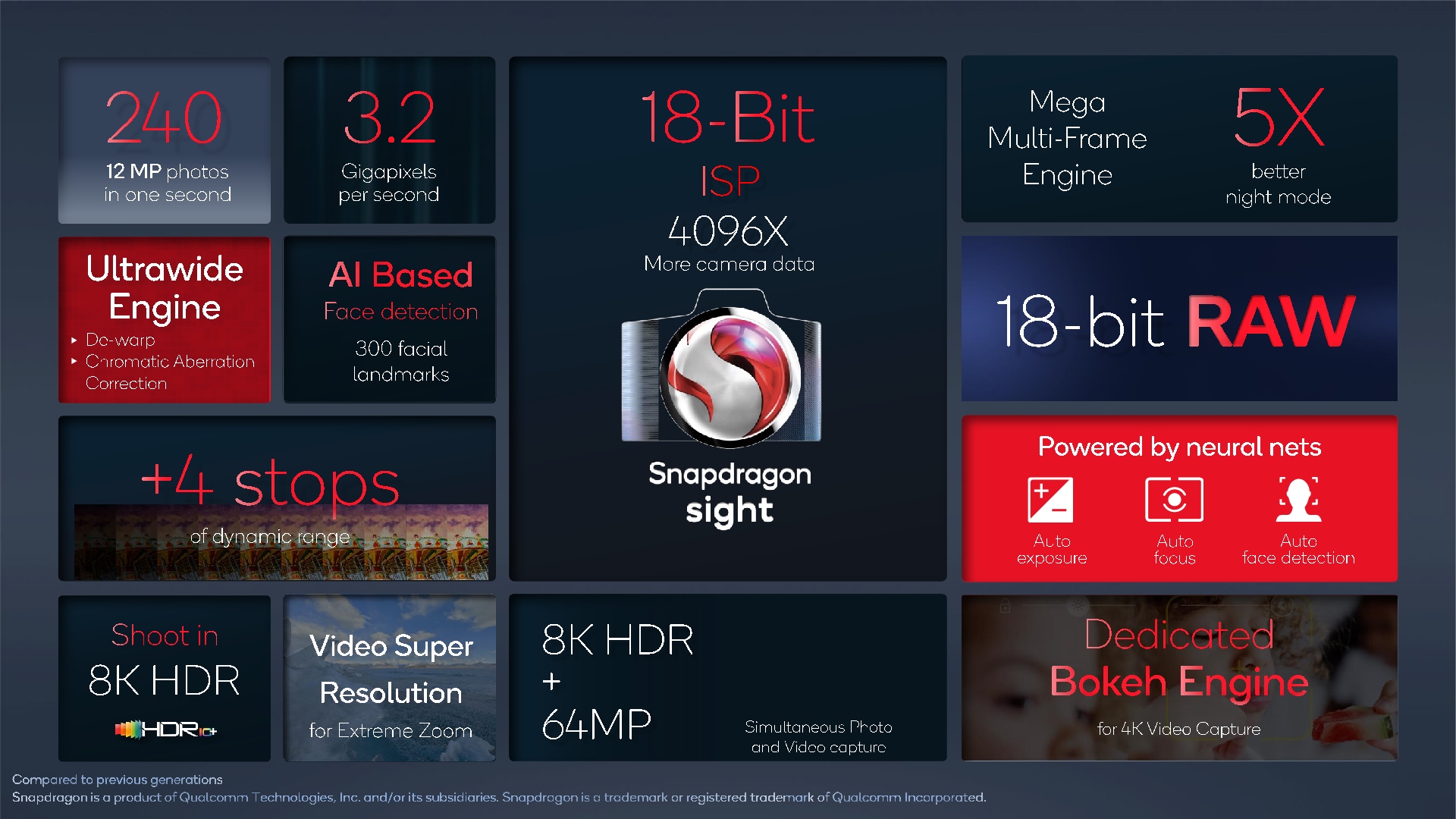
The big flagship feature being advertised is the fact that the new ISP is now capable of 18-bits of color depth per channel, up from the previous generation 14-bit ISP. While mobile image sensors nowadays still are barely 12-bit native in terms of their ADCs, the ushering of new HDR techniques such as staggered HDR capture, where exposures are immediately subsequent to each other on the sensor’s readout, means that new phones now are able to capture images a lot faster, recombining them into higher bit-depth results. Particularly here, the new 18-bit ISP pipeline now allows for three exposure HDR stacking off these new sensors.
The increased bit-depth should allow for an increase of 4 stops in dynamic range (or 2^4 = 16x the range), which greatly helps with very contrasting environments and challenging lighting situations. This is quite beyond any other camera solution right now, and being able to have this implemented in such a hardware fashion sort of blurs the line between traditional image capture techniques and the more software-defined computational photography methods of the last few years.
Indeed, the new ISP architecture seems to be very much a way to implement many of the existing computational photography techniques into fixed-function blocks: there’s a new neural-net controlled 3AA (auto-exposure, auto-focus, auto-white-balance) and face detection block, which sounds eerily similar to Google’s HDRnet implementations.
Night mode is also said to be vastly improved through a new multi-frame noise reduction and image stacking block, being able to now stack and align up to 30 images, and achieve also much finer detail this generation. Qualcomm here claims up to 5x better night mode shots.
Further improvements include a new distortion correction block that’s able to now also correct for chromatic aberrations, and a hardware video Bokeh engine, being able to operate at up to 4K video recording. Think of it as the same as the new Cinematic mode on the new A15 iPhones, but not only limited to 1080p.
Qualcomm notes that all the AI/ML/neural network features on the ISP are actually run and accelerated on the ISP itself, meaning that it is not offloaded onto the Hexagon dedicated ML processing blocks or the GPU.
Just as a note- Qualcomm’s 3.2Gigapixel/s throughput metric here seems low compared to the Dimensity 9000’s 9Gpixel/s, it’s possible that the companies are advertising very different metrics, with MediaTek advertising the throughput of lower-bit depth pixels coming from the image sensors per frame, while Qualcomm quoting the full bit depth pixel processing within the ISP itself.
In terms of video encoders and decoders, the new chip allows for 8K HDR recording now, but otherwise is seemingly on par with the Snapdragon 888 media blocks. Unfortunately, this also means no AV1 decoding this year yet again. Qualcomm isn’t part of the Alliance for Open Media consortium and instead is backing VVC/H.266 and EVC, however with AV1 being actively pushed by Google and YouTube, and seeing large adoptions such as by Netflix, it’s becoming questionable for Qualcomm to still not support the format in 2022 devices.
AI Performance - Iterative, but solid
Last year’s Hexagon IP block was a very large change for the Snapdragon 888. At the time, Qualcomm moved on from a more segregated DSP/AI architecture to a single more fused-together block being able to operate on scalar, vector, and tensor operations at the same time. This year’s iteration is an improvement of that larger change. Qualcomm notes that amongst many changes, they’ve doubled up on the shared memory of the block, allowing for greater performance for larger ML models (which are growing at a very fast pace).

Qualcomm didn’t note any TOPS figures this time around, instead stating we’re seeing 2x the tensor throughput performance, and smaller increases for scalar and vector processing. They do quote a day-1 to day-1 performance increase of 4x when compared to the Snapdragon 888, via a combination of both hardware and software improvements, but of course that figure is smaller when comparing both platforms on an equal software footing.
Power efficiency for AI workloads is said to be 70% better this generation, which is actually more significant, and should help with more demanding sustained ML workloads.
X65 Modem Integrated
In terms of connectivity, the Snapdragon 8 Gen 1 is quite straightforward, as it integrates the X65 modem IP that Qualcomm had already announced as a discrete model earlier this year.
The improvements here are the fact that it’s a 3GPP Release 16 compatible modem, including new features such as uplink carrier aggregation. Other improvements are 300MHz of Sub-6 bandwidth on 3 100MHz carriers, and an increase of the mmWave bandwidth from 800 MHz to 1000MHz, allowing a new peak theoretical downlink speeds of 10Gbps.


219 Comments
View All Comments
brucethemoose - Wednesday, December 1, 2021 - link
As far as laptops go, I think Qualcomm is betting the farm on those upcoming Nuvia cores.Unashamed_unoriginal_username_x86 - Tuesday, November 30, 2021 - link
QC pointing out that the ISP can now do all photo/video AI processing on its own seemed strange in the context of your previous statement about Apple using their GPU effectively in computational photography. I'm guessing it allows for better power gating/efficiency?mode_13h - Wednesday, December 1, 2021 - link
Or, maybe it's just them trying to spin a weakness into a strength.I had a similar thought. If they effectively fused all of their GPU compute + AI + signal processing, they might deliver more performance on each, while lowering SoC prices (or at least improving their margin) due to smaller area.
In truth, not that much separates DSP and GPU cores. For AI, Nvidia showed how you can bolt on some tensor multipliers and still feed them from the same GPU register file.
michael2k - Wednesday, December 1, 2021 - link
I assume there is better efficiency in having dedicated hardware blocks from the ISP in the pipeline rather than GPGPU blocks in the pipeline.There may be ISP dedicated RAM/cache. Apple has a 32MB system cache that I imagine is used by the GPU for image processing. Qualcomm only has a 4MB system cache, so it would make sense if the ISP has dedicated memory.
If that were the case then it also makes sense that shuttling data from and to the 4MB system cache for the GPU to use back to the ISP cache for the ISP to use would be computationally and power-wise expensive. Apple would avoid that kind of inefficiency because they would allow the ISP and GPU to both access the same 32MB system cache.
If the ISP already has access to the 4MB system cache then I don't see any reason to avoid using the GPU, unless the Adreno GPU is poorly suited for GPGPU. It might also just be that Qualcomm is licensing hardware blocks that don't integrate as well since they don't design them the way Apple claims to, and Apple can have multiple cooks in the kitchen as it were between the ML blocks, the NE blocks, the ISP block, and the GPU blocks all working on the same set of memory during photo and video workflows.
name99 - Thursday, December 2, 2021 - link
Isn't this a rerun of GOU fixed function blocks (which were killed by programmable shaders)?Sure, if you can be ABSOLUTELY CERTAIN than you know everything your camera will want to do, you can freeze than in the ISP. But doing the work on a more programmable block (some combination of GPU and NPU) leaves you able to retrofit a new idea in two years that you haven't even thought of today.
Ultimately it probably boils down to split responsibility.
Apple has the camera SW and HW teams working together.
QC has the problem (for better or worse) that it has no idea what Google will be doing with cameras in two years, and no strong incentive to ensure that the chip they sell today matches Google's requirements in two years.
A more interesting aspect is that for Apple's scheme (multiple IP blocks all working together) you need a NoC that can tag requests by QoS (for appropriate prioritization) and by stream (to aggregate locality). Apple certainly does this. The academic literature has plenty of discussion as to how this should be done, but I am unaware of the extent to which anyone in industry apart from Apple does this. Is this part of the standard ARM IP model? Is it something each SoC vendor does in their own way but they all do it differently?
mode_13h - Friday, December 3, 2021 - link
> doing the work on a more programmable block (some combination of GPU and NPU)> leaves you able to retrofit a new idea in two years that you haven't even thought of today.
It's (usually) also a boon for code maintenance, if you can implement features in a similar way, across multiple generations of hardware. Programmable engines (call them DSP, ISP, GPU, or what you will) are the way to do this, with the caveats that there are inevitably hardware bugs and other quirks that need to be worked around in a generation-dependent manner, and that this approach poses additional challenges for realtime (i.e. video), due to shifting performance characteristics and amounts of resources.
mode_13h - Friday, December 3, 2021 - link
> you need a NoC that can tag requests by QoS (for appropriate prioritization)> and by stream (to aggregate locality).
Only realtime apps truly need that. And of those, all that come to mind are video processing and AR. I'd say AR might've been the real driver, here. Sure, audio processing is also realtime, but tends to be so much lower-bandwidth that it wouldn't be as dependent on realtime scheduling.
name99 - Monday, December 6, 2021 - link
Apple was tagging content on the SoC by QoS and stream back with the A4. It's not something new.And "realtime" is somewhat flexible. Of course video capture is hard realtime, but even screen animation effects are soft realtime. You mock this as unimportant, but iPhones have been distinguished by the smoothness of their animation, and general lack of visual/touch glitching, from day one (remember Project Butter and all that?)
mode_13h - Tuesday, December 7, 2021 - link
> You mock this as unimportant,Huh? Where? I respect rock-solid, smooth animations and consistently good responsiveness.
I'm not convinced that warrants QoS tagging of associated bus transactions, but that's only because you don't want UI animations to be particularly taxing, for the sake of battery longevity. If they're not, then it should be enough for the OS scheduler to prioritize the supporting CPU & GPU threads.
name99 - Tuesday, December 7, 2021 - link
How do you think prioritization is IMPLEMENTED at the point that it hits that hardware?Any particular NoC routing point, or the memory controller, or any other shared resources has to decide who gets access in what order.
OS scheduling doesn't help here! All OS scheduling has done is decide which code is currently running on which CPU (or GPU), and that code won't change for 10ms (or whatever the scheduling granularity is). If you want the hardware to make better choices (do I prioritize the requests coming from a CPU or the requests coming from the ISP?), it needs to know something about the packets flowing through the router and the requests hitting the memory controller -- which are low latency, which can be delayed so much but no more, which are best effort.
That's what tagging (by QoS and stream) achieve!
In the absence of such tags, the best you can do is rely on
- heuristics (which are never perfect, and frequently far from perfect)
- massive overprovision of HW (which is sub-optimal in a phone; and never works anyway because demands always expand given that the HW can [to 95th percentile, anyway...] kinda sorta support the new demands. )