AMD CPUs in 2022: Zen 4 in Second Half, Ryzen 7 5800X3D with V-Cache by Spring
by Dr. Ian Cutress on January 4, 2022 10:42 AM EST
One of the things I look forward to every year is whether the major companies I write about are prepared to showcase their upcoming products in advance – because the year starts with the annual CES trade show, this is the perfect place. A company that’s able to present its 12-month portfolio comes across as confident in its ability to deliver, and it also gets the rest of us salivating at the prospect of next-generation hardware. This time around AMD steps up to the plate to talk about its new V-Cache CPU coming soon, and its new Zen 4 platform coming in the second half of the year.
Now with V-Cache! One Sole CPU: Ryzen 7 5800X3D
Every CPU has levels of internal memory, known as cache, which starts as a bank of ‘Level 1’ fast but small memory, rising up to a ‘Level 2’ medium-sized medium speed memory, and then a ‘Level 3’ larger sized slower memory. Beyond this there’s the main DDR memory, which is super big, but super slow in comparison – main memory is 100x slower to access, but can hold a lot more data.
Last year AMD announced that it had been working on stacked onboard memory in the form of cache. This V-Cache concept took one of the standard 8 core chiplets from the Ryzen 5000 series, which already had 32 MB of L3 cache, and stacked on top of it another 64 MB of L3 cache, giving a total of 96 MB. Stacking chips is difficult, and AMD has been working with TSMC to productize this advanced packaging technique.
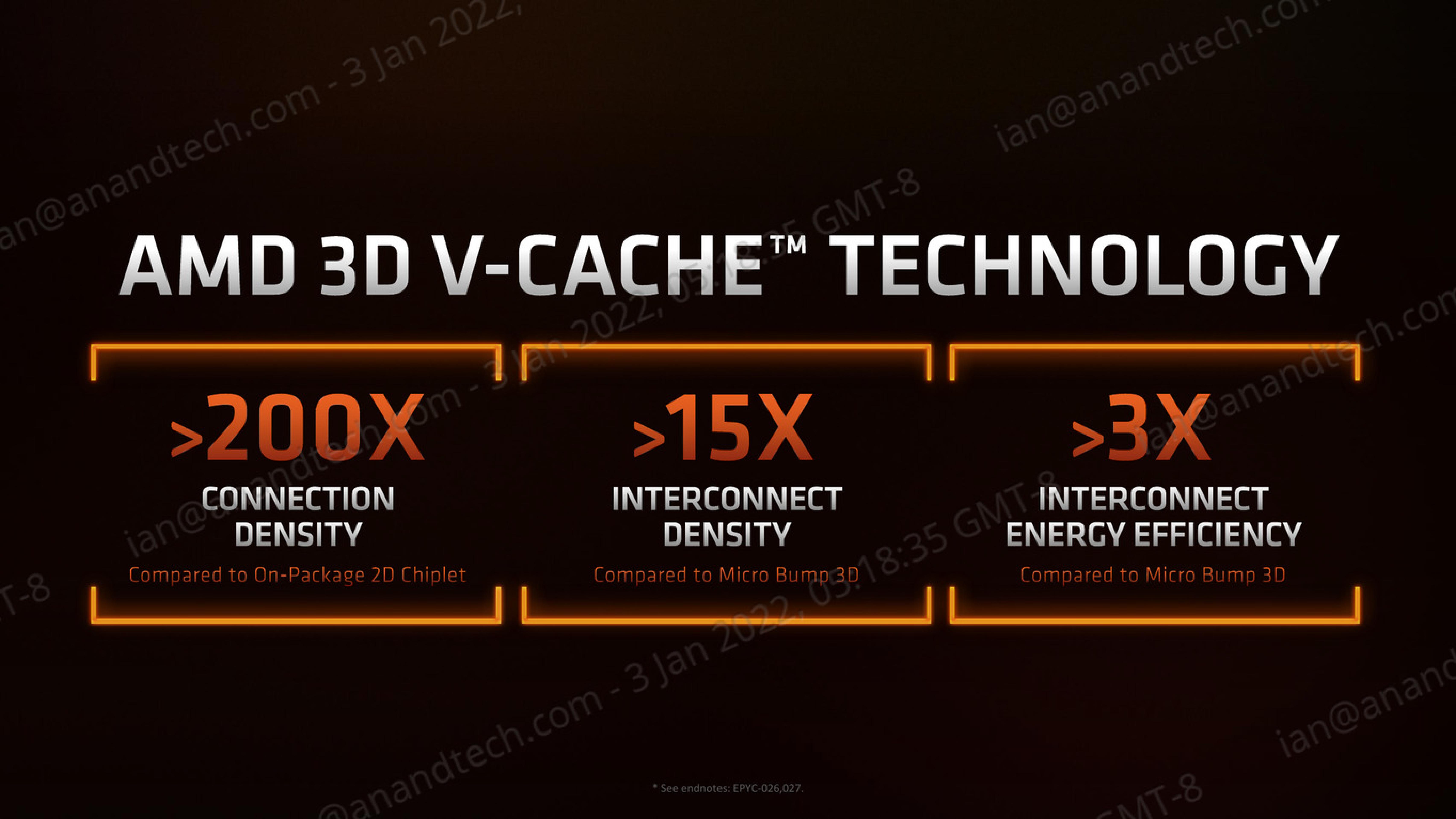
The main 8-core chiplet, built on TSMC 7nm, measures 82 mm2. This extra stacked chiplet is only 36 mm2, and sits directly above the cache already on the chip, so it does not cover the cores. The extra 64 MB of L3 cache chiplet is manufactured on a version of TSMC 7nm that is optimized for cache density, and so AMD has placed 64 MB on top of 32 MB directly. The cores are not covered for thermal reasons – the cores are where the power is used, and so thermal spaces are placed on top to make the top of the combined chip fully flat.
AMD stated last year that it would be manufacturing consumer and enterprise versions of this increased cache in 2021 for launch in 2022. At the Data Center event last year in November, AMD announced the version that would go into servers, and called it Milan X. For consumers, AMD is announcing today what this increased cache version of Ryzen looks like. Introducing, the Ryzen 7 5800X3D.
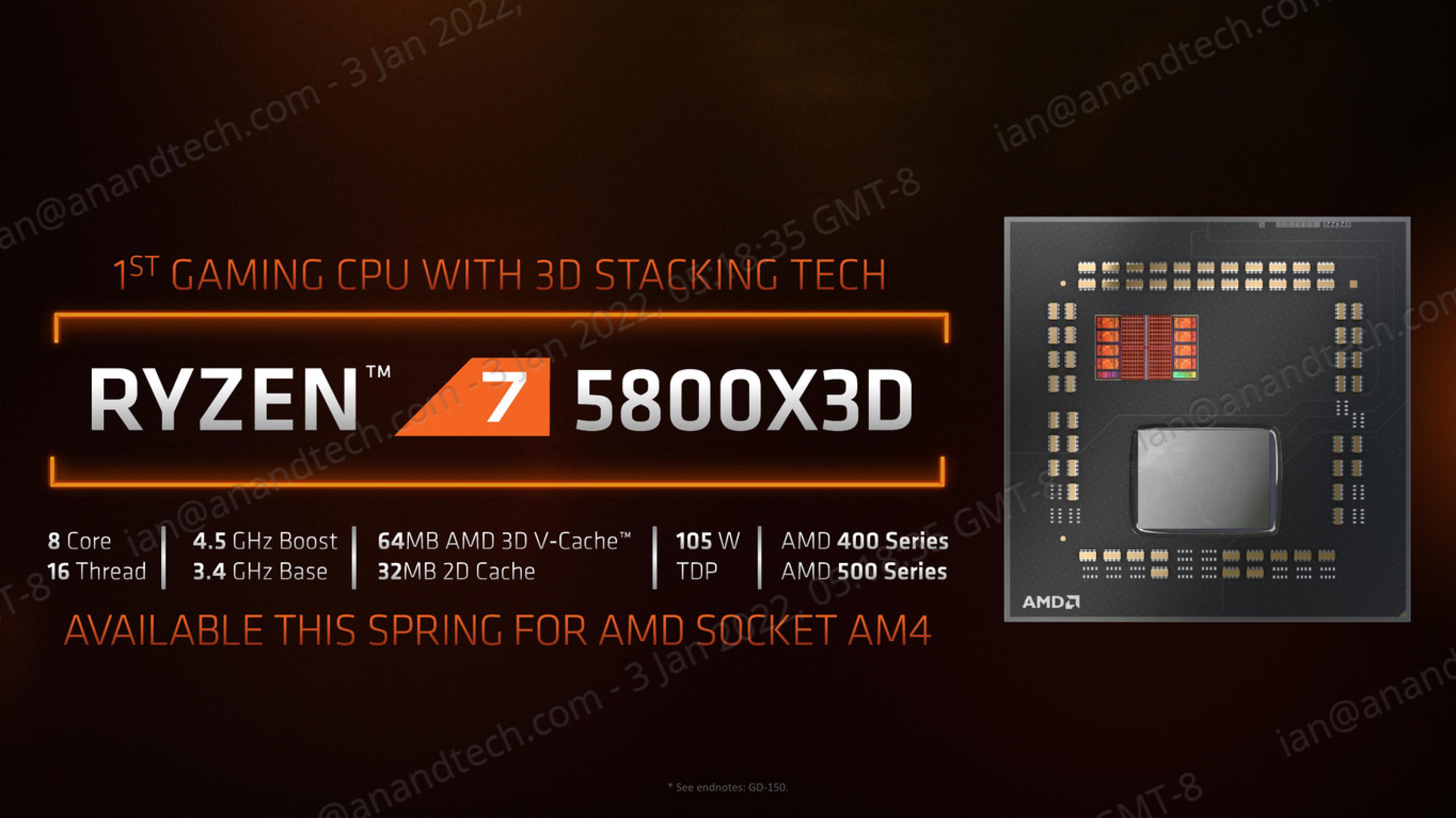
AMD is only going to launch a single Ryzen version of its V-Cache technology, using the Ryzen 7 5800X as a base. This means the chip is 8 cores, 16 threads, and 105 W TDP just like the regular R7 5800X, but with 96 MB of L3 cache now rather than 32 MB. It will run at 3.4 GHz Base, 4.5 GHz boost, be overclockable, and work in AMD 400-series and 500-series motherboards.
| AMD Ryzen 5000 Series Processors for Desktop Zen 3 Microarchitecture (Non-Pro, 65W+) |
|||||||||
| AnandTech | Core/ Thread |
Base Freq |
1T Freq |
L3 C$ |
IGP | PCIe | TDP | SEP | |
| Ryzen 9 5950X | 16 | 32 | 3400 | 4900 | 64 MB | - | 4.0 | 105 W | $799 |
| Ryzen 9 5900X | 12 | 24 | 3700 | 4800 | 64 MB | - | 4.0 | 105 W | $549 |
| Ryzen 9 5900 | 12 | 24 | 3000 | 4700 | 64 MB | - | 4.0 | 65 W | OEM |
| Ryzen 7 5800X3D | 8 | 16 | 3400 | 4500 | 96 MB | - | 4.0 | 105 W | ? |
| Ryzen 7 5800X | 8 | 16 | 3800 | 4700 | 32 MB | - | 4.0 | 105 W | $449 |
| Ryzen 7 5800 | 8 | 16 | 3400 | 4600 | 32 MB | - | 4.0 | 65 W | OEM |
| Ryzen 7 5700G | 8 | 16 | 3800 | 4600 | 16 MB | Vega8 | 3.0 | 65 W | $359 |
| Ryzen 5 5600X | 6 | 12 | 3700 | 4600 | 32 MB | - | 4.0 | 65 W | $299 |
| Ryzen 5 5600G | 6 | 12 | 3900 | 4400 | 16 MB | Vega7 | 3.0 | 65 W | $259 |
| Ryzen 3 5300G | 4 | 8 | 4000 | 4200 | 8 MB | Vega6 | 3.0 | 65 W | OEM |
The processor will launch in the Spring (March/April we think), and exact pricing is yet to be announced.
For those that have been following AMD’s V-Cache news over this past year, I bet you have exactly the same questions I did when AMD first briefed us on this announcement. Here is a summary of the questions I asked, and my interpretations of the responses.
Why only Ryzen 7, not Ryzen 5/Ryzen 9? Because this is a new project for AMD, they want to find out how a processor like this will be welcomed into the market. A lot of users (myself included) expected AMD to go all-in with a big 16-core version, however anything Ryzen 9 requires two chiplets, and adding the extra V-Cache does require an extra cost in silicon and packaging. During a semiconductor shortage, I was told that this is the best way to get it into the hands of many people while also not in the super high-cost bracket. It also means one single unified 96 MB of L3 cache, without having to deal with two chiplets worth which might not be optimized immediately. Future versions of V-Cache on next-generation products may be expanded to other Ryzen members of the family.
The frequencies are lower than the regular 5800X? The cache does add a few watts to the power both in terms of idle and load. Rather than bin a stricter chiplet, the decision was made to reduce the frequency a little, but still allow overclocking. The chip, while listed at 105 W, still has the 142 W package power tracking for motherboards that support it.
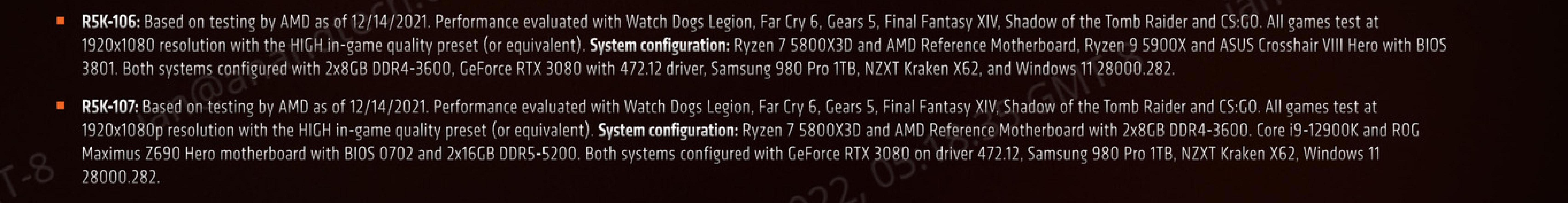
Who is this chip for? The focus is on users playing video games over anything else. The extra cache is meant to help with communications with discrete graphics cards, offering additional performance above the regular R7 5800X. Productivity workloads are less likely to be affected, and for those users the regular Ryzen CPUs are expected to be better. The Ryzen 7 5800X3D is designed to be the ‘World’s Fastest Gaming Processor’ (when compared to the 5900X and 12900K).
In terms of those performance metrics, AMD is quoting:
- From 1.0x to 1.4x at 1080p High vs Ryzen 9 5900X + RTX3080 (15% average)
- From 0.98x to 1.2x at 1080p High vs Core i9-12900K (DDR5) + RTX3080
Both systems were running Windows 11.
The critical element here I think is going to be the price. As I’m writing this piece, I can find the following prices:
- Ryzen 5 5600G (6C/12T*): $240
- Ryzen 5 5600X (6C/12T): $290
- Core i5-12600K (6P+4E*): $300
- Ryzen 7 5700G (8C/16T*): $340
- Ryzen 7 5800X (8C/16T): $369
- Core i7-12700KF (8P+4E): $390
- Ryzen 9 5900X (12C/24T): $540
- Core i9-12900KF (8P+8E): $590
- Ryzen 9 5950X (16C/32T): $730
Even though AMD is promoting the Ryzen 7 5800X3D to be higher performance than the 5900X in gaming, if it goes anywhere north of $500, it might be badly received. At $500, it would be a +$130 add-on from the regular Ryzen 7 5800X. Are users willing to pay almost 30% more for triple the L3 cache for up to 15% more performance in gaming? Or is this just simply a play for the world’s fastest gaming processor, regardless of cost?
Don’t get me wrong here, I think the technology is great. But in order for AMD to keep the same margins, it might be more expensive than people think. I’m looking forward to getting it in hand for review – let us know what sort of tests you want to see.
Coming 2H 2022: Zen 4 on 5nm, with AM5, DDR5, and PCIe 5.0
Perhaps not that surprising given all the information from last year, AMD has confirmed that Zen 4 based Ryzen CPUs coming in 2022 will be built on TSMC’s 5nm process (we assume N5), will be built on the AM5 socket, and feature DDR5 as well as PCIe 5.0. What we get new out of this disclosure are images of the new socket, and a render of the CPU form factor.
With AM5, AMD is going to move to a Land Grid Array (LGA) style of processor, similar to Intel, eliminating the Pin Grid Array (PGA) that has been used on the current Ryzen desktop processors. AMD is no stranger to LGA, given that its EPYC enterprise processors and Threadripper processors both use it. The new AM5 socket is a 1718 pin design, with the pins in two orientations:
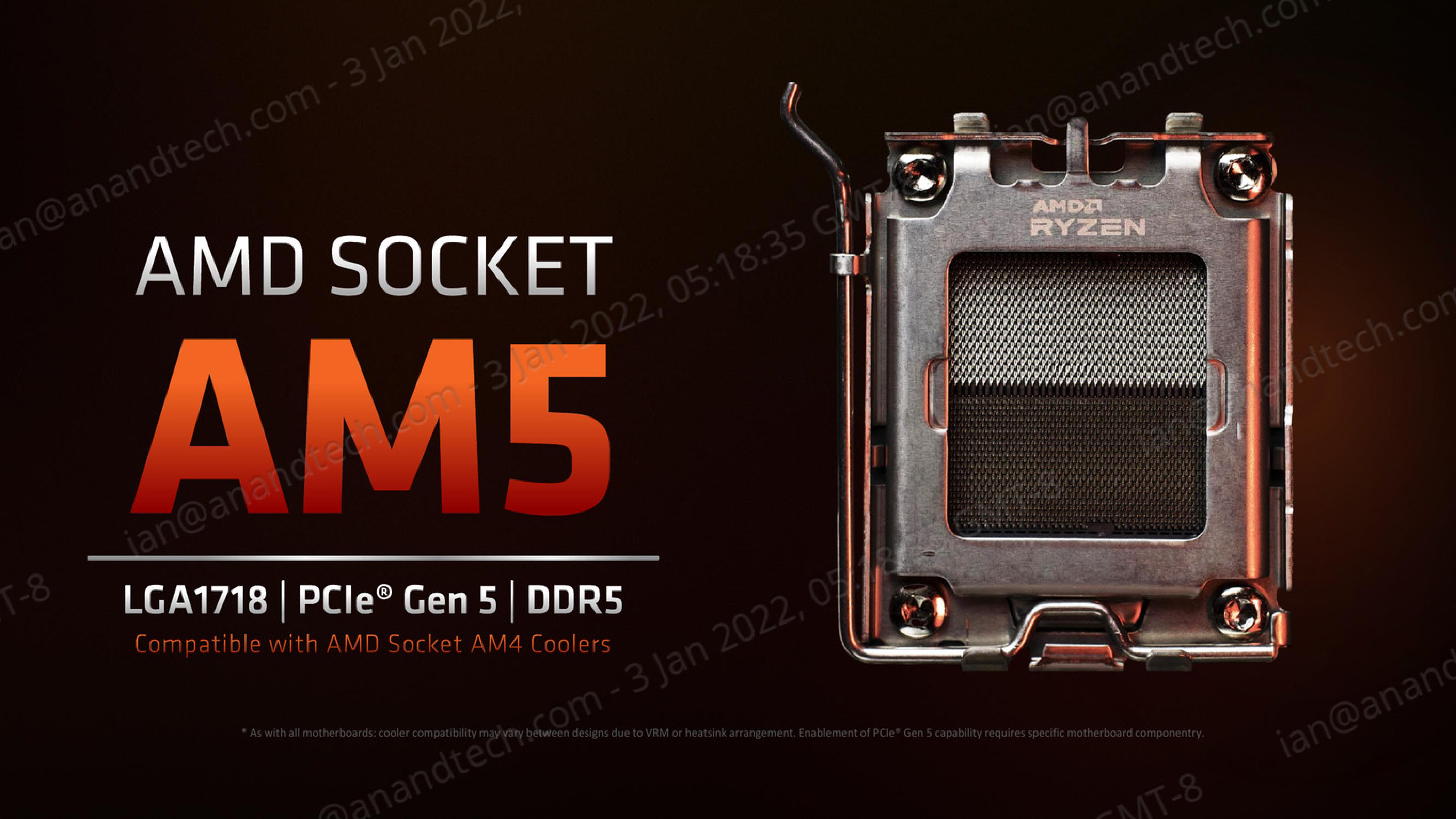
If this sort of socket looks familiar to any of you, it’s because it appears to be a denser version of AMD’s old socket F back in 2006-2010. While that old socket at 1207 pins for Opteron enterprise processors, this one has 1718, so you’ll see us refer to it as LGA1718. Compared to Intel’s 12th Gen Core processors that use an LGA1700 socket, both the major platforms are around the same number of pins.
It is worth noting that this sort of socket, like the old Socket F, means that the bottom of the Zen 4 processors will be nothing but contact pads. The use of an LGA socket means the pin density is defined at the socket level, rather than on the processor, and it’s easier to design a socket with a higher pin density. But the pin-only rear means that some of the power circuitry for the chip will be both in-package and on the top, which is handy given that AMD is also showcasing what the CPU will look like.
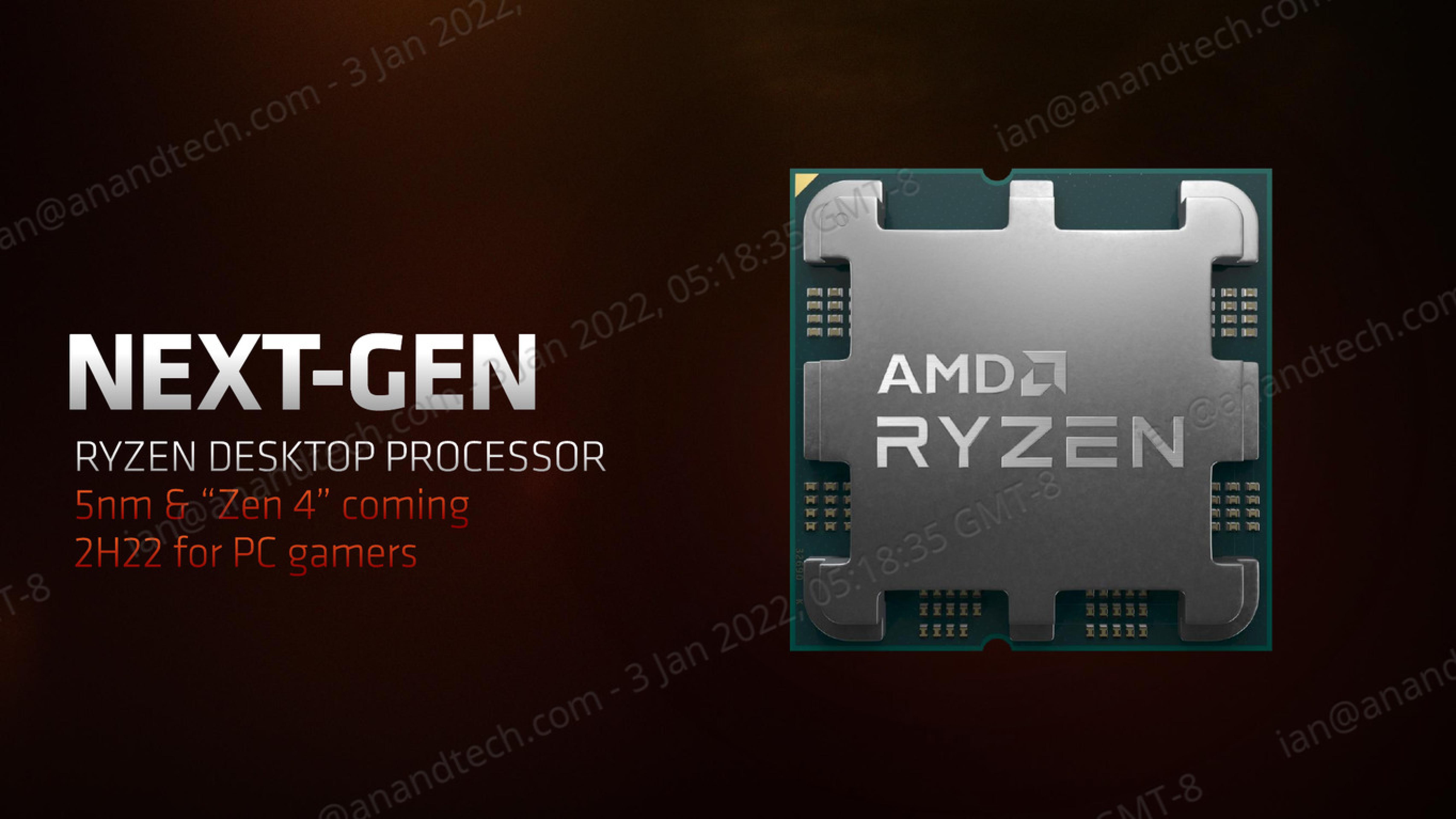
We’ve got another square-like CPU package, however to accommodate some of that power delivery the heatspreader has this sort of octopus arm design to it. The heatspreader is not rotationally symmetric, with the top/bottom (as shown) central arms being smaller than the left/right central arms. The processor also has two notches, one at the top and one at the bottom, just left of center to make sure that the processors are entered in the right way. There’s also that yellow arrow on the top left corner to help guide the user.
On top of showcasing the CPU and the LGA1718 socket, AMD is confirming that the AM5 platform will support AM4 coolers. This means we should expect the mounting holes for AM5 to be the same, or at least the platform to accept both old and new.
Next-Gen Ryzen, featuring Zen 4 cores, 5nm manufacturing, and the new AM5 socket, is coming to market in the second half (2H) of 2022. Core counts and everything else will come later – I suspect we’ll get a deep dive into the architecture sometime around August, at the Hot Chips industry event, or at a special AMD event around that time.


99 Comments
View All Comments
Mike Bruzzone - Sunday, January 16, 2022 - link
Intel component and mobile U stuck on the shelf is the primary reason for regional pricing problems. Rocket deadweight, Comet S down bin, Coffee Refresh single thread, Tiger, Ice, Comet U quad laptops are on fire sale. Inflated dGPU card price is paying for channel's Intel inventory financial write down and/or loss. Worst is retail CPU + GPU and board kit deal where inflated GPU card price offsets the CPU loss leader and the board add its own mark up. There is no x86 or GPU card shortage data can validate it's called capital creation on channel Intel surplus inventory financial risk management. mbMike Bruzzone - Sunday, January 16, 2022 - link
Package area for pulling off the heat and material composition is not TR and Epyc Fujitsu composite? I think so. 59003D was always a lid off lab demo? I think so. mbSpunjji - Wednesday, January 5, 2022 - link
"They put something out to try and take headlines away from Alder Lake because they do not have anything of note until Zen 4 releases later this year."You might have missed how this was previewed months back? AMD and TSMC don't go through months and months of design and validation to chuck out something to mess with publicity for one of Intel's products. The technology will mostly benefit AMD's server division, but they promised something for the gamers and here it is, for better or worse.
Mike Bruzzone - Tuesday, January 18, 2022 - link
Rembrandt appears AMD 2020'mainstay 'consumer' and mass market gaming product between the two suspension bridge towers of 3D and Zen 4. Rembrandt is the deck. Then imagine an arch from tower 1 abutment reaching height at mid span and then back down to tower two abutment is commercial gross margin lift; TR 5K, Epyc where Genoa is already shiping on AMD loss of 7 nm cost : price / margin advantage vis a vis Intel on TSMC foundry market up and commercial GPU which AMD is now focusing getting out from in between Intel and Nvidia in the consumer market. mbkwohlt - Wednesday, January 5, 2022 - link
To be completely fair, given timelines of CPU design, Alder Lake design began almost immediately after Zen 1 was released.Every CPU between Zen1 and now that Intel released felt like a half-assed retort because all they could do until Alder Lake was finished was convert their HEDT line to their consumer socket, cut prices, and crank the wattage to extreme levels.
lmcd - Saturday, January 8, 2022 - link
Began after Zen 1???? You're crazy. The Alder Lake plans started way before that. Intel has been iterating their Atom cores for this moment literally since 2013. The Apple A7 was Intel's wakeup call, architecturally. And yes, it takes that long to turn around a giant in an industry where design to tapeout is usually ~5 years, and Atom was way beyond just one product cycle from reaching the necessary performance characteristics.Up until the A7, Intel assumed it could meet Apple on Apple's newfound turf. With the A7, Intel canned their smartphone product plans almost instantly and pivoted Atom toward its current trajectory. The only reason Alder Lake took quite this long is because of Intel's foundry slips.
Spunjji - Monday, January 10, 2022 - link
"The Alder Lake plans started way before that"Is there any evidence for that? I could believe they had some blue-sky ideas floating around about it, but given your quoted 5 years from design to tape-out the idea that Alder Lake is a direct response to Zen makes perfect sense.
Mike Bruzzone - Sunday, January 16, 2022 - link
Intel had disaggregate dice in desktop MCM parallel Core Haswell and Rad hard MCM SIP launched into space decades ago. mbSpunjji - Wednesday, January 5, 2022 - link
"The trade-off is more frequency or more cache"Unless you're already at the limit for frequency, then you'd just get more cache (and a little more power draw).
"Also, I'm sure the stacked die reduces the ability to dissipate heat"
Sure - from the cache. It's not stacked on top of the cores where most of the heat comes from.
nandnandnand - Tuesday, January 4, 2022 - link
If the Epyc Milan-X numbers are anything to go by, it's more impressive for non-gaming use cases.