Universal Chiplet Interconnect Express (UCIe) Announced: Setting Standards For The Chiplet Ecosystem
by Ryan Smith on March 2, 2022 8:30 AM ESTIf there has been one prominent, industry-wide trend in chip design over the past half-decade or so, it has been the growing use of chiplets. The tiny dies have become an increasingly common feature as chip makers look to them to address everything from chip manufacturing costs to the overall scalability of a design. Be it simply splitting up a formerly monolithic CPU in to a few pieces, or going to the extreme with 47 chiplets on a single package, chiplets are already playing a big part in chip design today, and chip makers have made it clear that it’s only going to grow in the future.
In the meantime, after over 5 years of serious, high-volume use, chiplets and the technologies underpinning them seem to finally be reaching an inflection point in terms of design. Chip makers have developed a much better idea of what chiplets are (and are not) good for, packaging suppliers have refined their ultra-precise methods needed to place chiplets, and engineering teams have ironed out the communications protocols used to have chiplets talk amongst each other. In short, chiplets are no longer experimental designs that need to be proven, but instead have become proven designs that chip makers can rely on. And with that increasing reliance on chiplet technology comes the need for design roadmaps and stability – the need for design standards.
To that end, today Intel, AMD, Arm, and all three leading-edge foundries are coming together to announce that they are forming a new and open standard for chiplet interconnects, which is aptly being named Universal Chiplet Interconnect Express, or UCIe. Taking significant inspiration from the very successful PCI-Express playbook, with UCIe the involved firms are creating a standard for connecting chiplets, with the goal of having a single set of standards that not only simplify the process for all involved, but lead the way towards full interoperability between chiplets from different manufacturers, allowing chips to mix-and-match chiplets as chip makers see fit. In other words, to make a complete and compatible ecosystem out of chiplets, much like today’s ecosystem for PCIe-based expansion cards.

Chiplets in a Consumer Processor - Both Dense and Sparse
The comparisons to PCIe are apt on multiple levels, and this is perhaps the best way to quickly understand the UCIe group’s goals. Not only is the new standard being made available in an open fashion, but the companies involved will be establishing a formal consortium group later this year to administer UCIe and further develop it. Meanwhile from a general technology perspective, the use of chiplets is the latest step in the continual consolidation of integrated circuits, as smaller and smaller transistors have allowed more and more functionality to be brought on-chip. In essence, features that have been on an expansion card or separate chip up until now are starting to make their way on to the chip/SoC itself. So like PCIe moderates how these parts work together as expansion cards, a new standard has become needed to moderate how these parts should work together as chiplets.
Ultimately, the stated goal of the groups behind UCIe is to establish an open and ubiquitous ecosystem for chiplets. Whether that means simply standardizing some of the physical aspects for easier manufacturing, or enabling a true mix-and-match setup where clients can request a chip built with chiplets from multiple chip(let) makers, a strong underlying standard is needed to make this happen. And the major players in the chipmaking industry are throwing their weight behind UCIe to make this happen.
Why Chiplets?
The underlying rationale for all of this, in turn, is the increasing use of – and in some cases, outright need for – chiplets. Chiplets are already being used to mix dies from multiple chipmakers or from multiple process nodes, and they’re being used to build large chips that otherwise wouldn’t be possible due to reticle limits. All of which is being driven by either economics in some fashion (not using an expensive, bleeding-edge node for every part of a chip), or a desire to combine IP from disparate manufacturers in a more expedient fashion than spending years taping out a monolithic chip. To be sure, monolithic chips as a whole aren’t going away entirely (moving data remains expensive), but the economics of chip design are inexorably driving the use of chiplets in more cases.
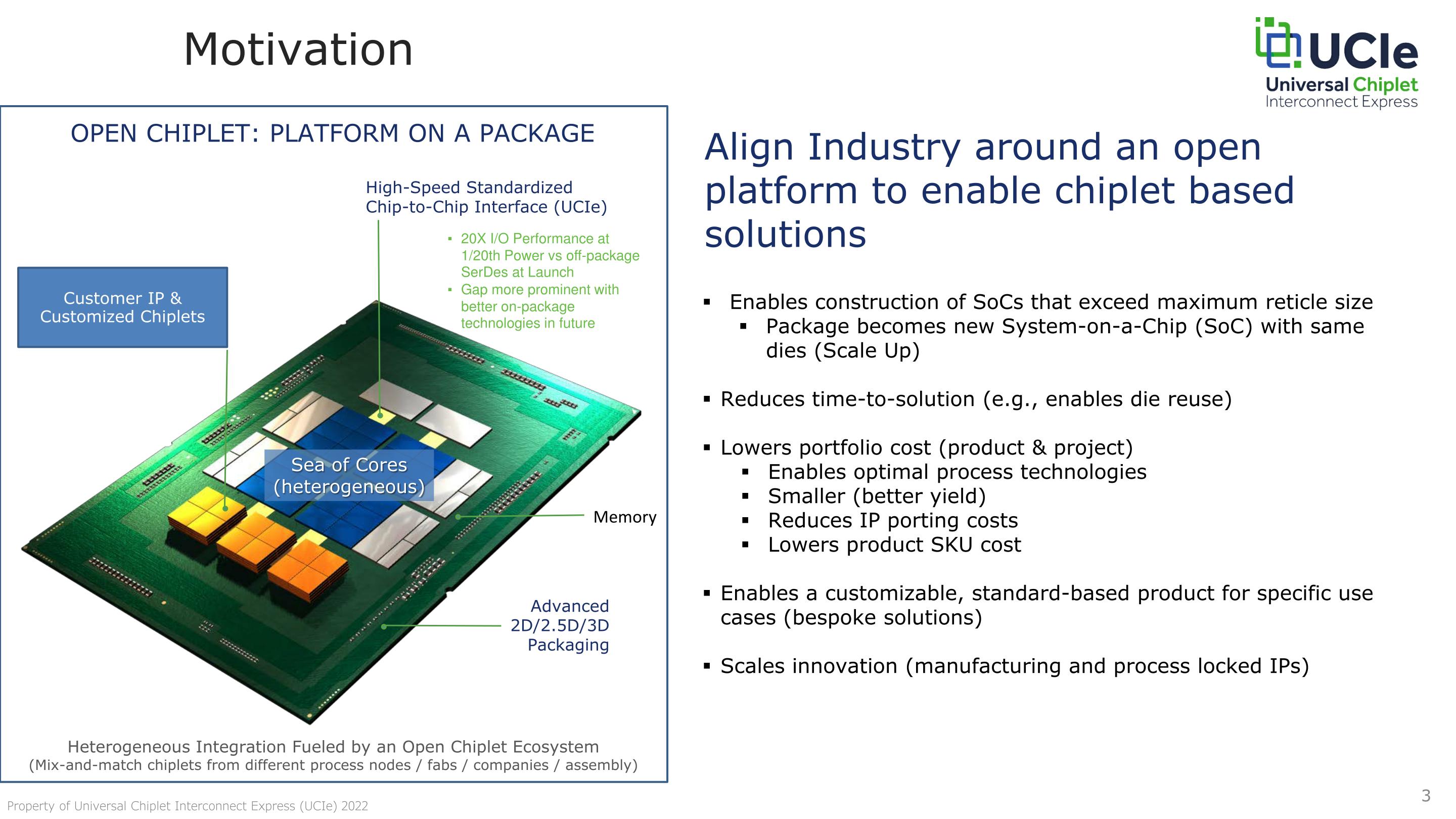
Meanwhile there is also a push for performance and efficiency that is driving the ongoing interest in chiplets. Or to be more specific, driving a desire to integrate more functions on to a single chip package. PCIe, for as quick as it is, is still slow by chip standards; the long trace lengths from a CPU to a controller (and back again) add up to a lot of latency, and pushing data around that far is relatively expensive in terms of power. So chip makers are increasingly wanting to bring those functions on chip, to bring down latencies and cut down on power consumption. Which in the case of chiplets (and thus UCIe) means being able to improve performance by upwards of 20x and reducing power consumption by roughly the same amount.

UCIe 1.0: New Die-To-Die Spec with PCIe & CXL Layered on Top – Available Today
Diving into the first revision of the UCIe specification, we find something that’s pretty straightforward, and something that’s very clearly designed around the capabilities of today’s packaging technologies. What UCIe is bringing to the table today isn’t so much new technologies as it is standardization between the different implementations of current technologies, so that everyone has a common ground to work with.
Perhaps not too surprisingly, this initial version of UCIe comes from Intel, who is donating the specification wholesale to the industry and what will become the UCIe consortium. Intel has been responsible for the initial development of several high-profile open interconnect technologies over the decades – not the least of which has been USB, PCIe, and Thunderbolt 3 – so it’s not too shocking to see them donating another interconnect technology to help kickstart what they (and the rest of the industry) believe to be the next wave of computing. Make no mistake, though, this isn’t an Intel-only initiative, as evidenced by the companies backing the new standard and who will be forming the upcoming consortium. (Whenever you have senior fellows from both Intel and AMD on the same briefing call, you know something big is going on)
Under the hood, UCIe borrows from Intel's earlier Advanced Interface Bus (AIB) technology. Intel previously donated that technology to the CHIPS alliance in 2020, so this is not the first time Intel has released a version of this technology in an open fashion. But UCIe is the largest (and most chiplet-focused) effort yet, as evidenced by the backing of Intel's fab rivals, as well as CPU design rivals.
As for the UCIe specification itself, let’s talk about what it does and doesn’t cover. The specification covers the physical layer, laying out the electrical signaling standards that chiplets will use to talk to each other, as well as the number of physical lanes and the supported bump pitches. And the specification covers the protocol layer, defining the higher-level protocols overlaid on those signals to make sense of everything and to provide the necessary feature set.
What the specification doesn’t cover, however, is the packaging/bridging technology used to provide the physical link between chiplets. This isn’t Intel giving away EMIB or Foveros, for example. Rather, UCIe is bridge-agnostic; chiplets can be linked via fanout bridge, silicon interposers, EMIB, or even just a plain old organic substrate in the case of lower bandwidth devices. UCIe is meant to work with all of these, as the bridge itself is essentially a dumb pipe to carry the electrical signals between chiplets. So long as a chiplet adheres to the standard (including bump pitch), then it will be able to talk to another UCIe chiplet.
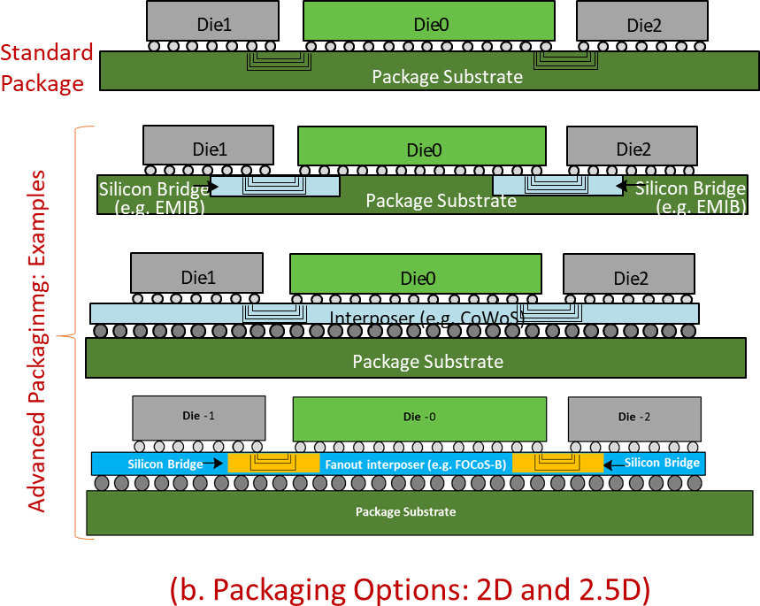
On that note, UCIe 1.0 comes with essentially two performance/complexity standard levels. The specifications for the aptly-named “standard package” level are designed for lower bandwidth devices that use traditional organic substrates. These parts will use up to 16 lanes of data, 100μm + bump pitches, and extended channel lengths. At a high level, it’s like hooking up two devices over a contemporary PCIe link, but placing them much, much closer.
Meanwhile a second set of specifications covers what the UCIe group deems “advanced package”, and this covers all of the high-density silicon bridge-based technologies like EMIB and InFO. The advanced package specification calls for smaller bump pitches – on the order of 25μm to 55μm – as well as 4x as many lanes per cluster owing to the greater density, and very short channel reaches of under 2mm. Which taken to its fullest configuration, the UCIe promoters believe that an advanced package setup using today’s 45μm bump pitch technology would be able to deliver up to 1.3TB/s/mm of shoreline (linear) bandwidth. That is to say, 1.3TB per second of data would be able to pass through a 1mm edge of a chip.

I won’t rattle off every single figure here, but all of this is meant to underscore how UCIe is being setup to serve chiplet needs at both ends of the performance spectrum. For chip makers who just need to get two chiplets together on a single package in a cost-effective manner, there’s the standard package approach. And for chipmakers who need to make two chiplets behave as close as possible to a single monolithic chip, the advanced packaging specifications allow for a lot of lanes – and thus a lot of bandwidth.
Meanwhile, it’s interesting to note just what the promoters are expecting in terms of latency and energy efficiency. For all package types, latency is expected to be under 2ns, which is especially critical in chiplet designs that are splitting up what would previously have been a monolithic chip design. Meanwhile power efficiency ranges from a low 0.5 pJ/bit for standard packaging, to an even lower 0.25 pJ/b for advanced packaging. This helps to illustrate just why some chipmakers are eager to get on board with chiplets, as the improvements over discrete PCIe/CXL cards could be significant.
The physical layer linking up chiplets, in turn, is new for UCIe. Intel and the other promoters aren’t going too deep into how this works (even in their whitepaper), but at a high level the physical layer standard provides for electrical signaling, clocking, link training, and sideband signaling. A 256 byte Flow Control Unit (FLIT) in turn handles the actual data transfer.
Above this is something of a half-way layer, which the group calls the Die-to-Die Adapter. The D2D provides the basis for link state management and parameter negotiation between chiplets. The D2D is also responsible for providing optional support for additional data reliability safeguards via CRCs and link-level retries.
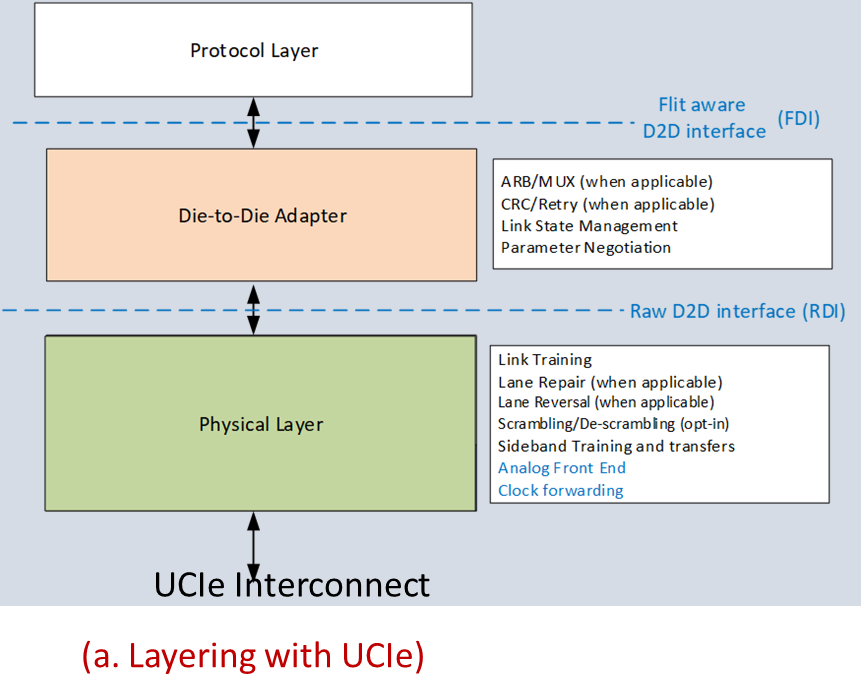
Finally, at the protocol layer, chiplet makers have a few different options. The official standardized protocols for UCIe are PCI-Express and its cache-coherent cousin, Compute Express Link, which is itself built on top of PCIe. In discussing their choice here, the UCIe promoters opted to take the pragmatic approach: there is already industry-wide support for PCIe and CXL, so rather than reinvent the wheel themselves, they are going to leverage the existing ecosystems at the protocol layer. This means that UCIe is hitting the ground running with a fully fleshed out and well proven protocol layer that can provide for reliable data transfer and link management, as well as extra bespoke features like cache coherency. And perhaps equally as important, it means customers and chipmarkers alike can leverage their existing software investments in PCIe/CXL, further simplifying the development process and getting UCIe-compliant chiplets out the door that much sooner.
In practice, I would have been far more surprised if UCIe didn’t leverage PCIe/CXL in this fashion. PCIe technologies have become the backbone of various other technologies, and the industry as a whole has moved past trying to out-invent PCIe when it comes to basic device interconnect needs.
That said, the promoters have made it clear that UCIe isn’t locked to just PCIe/CXL. Future versions of the standard may add other protocols if something comes along and the owner is willing to donate it to the standard.
Finally, chipmakers are also free to use their own custom/bespoke protocols as well; they are not restricted to using just PCIe/CXL. UCIe supports a raw/streaming protocol option that allows any other protocol to be used. Both chiplets would need to support this custom protocol to make a connection, of course, but even in this case, this would allow a chipmaker to leverage the physical aspects of the UCIe standard to simplify their own design/production.
That also means that existing interconnect protocols, such as AMD’s Infinity Fabric, aren’t likely to be going anywhere, even with the introduction of UCIe. Protocols like IF are still far more complex and specialized than what PCIe/CXL are capable of, which makes sense given the very specific coherency requirements for linking up CPU cores and I/O dies. Put another way, the very cutting edge of chiplet design remains ahead of where UCIe 1.0 is starting things off.
Going Long: UCIe For External Interconnects, As Well?!
And though UCIe is first and foremost focused on providing an on-chip interconnect for chiplets, the standard actually includes provisions for going off-chip. Way off-chip.
If a chip/system builder desires to, the specification allows for retimers to be used to transfer UCIe at the protocol level over much longer distances. This does, admittedly, sacrifice the latency and power benefits by virtue of adding (a lot of) distance. But the UCIe promoters envision server customers using this to provide UCIe connections at the rack or pod level, offering a direct chiplet-to-chiplet connection even over long distances.

The most interesting and most obvious use case for this kind of setup is silicon photonics. Extending the chiplet concept there, a chip maker could build a co-packaged optical transceiver on to the edge of a package, and then use UCIe to connect it to another chiplet. This would allow optical interconnection directly from the chip, bypassing the need (and power cost) of going to an off-chip transceiver.
The promoters are also showing off concepts based around external memory/storage devices. As well as external racks/draws with more SoCs on them.
UCIe 1.0 Is Just the Beginning
While the UCIe 1.0 specification is being released today, the promoters behind the standard are already turning their eye to the future of the technology, and of the consortium itself.
UCIe 1.0 is very much a “starting point” standard, which comes from being originally developed in a solo fashion inside of Intel. As previously mentioned, the consortium will be looking at other possible protocols to add to the standard. And thus far, the standard is only defining two of what they consider to be four aspects of chiplet design: the physical layer and the communication protocols. The group would like to go further in making a mix-and-match chiplet ecosystem a reality by also defining standardized chiplet form factors, and even managing other chiplets.
This is on top of ongoing changes in chip packaging technologies, which are still progressing. The UCIe 1.0 standard is essentially only defined for 2D and 2.5D chip packaging, but not 3D direct die-to-die technologies like the forthcoming Foveros Direct. As 3D chip packing becomes available, the standard will need to be updated to account for the new capabilities offered, as well as the even greater densities.
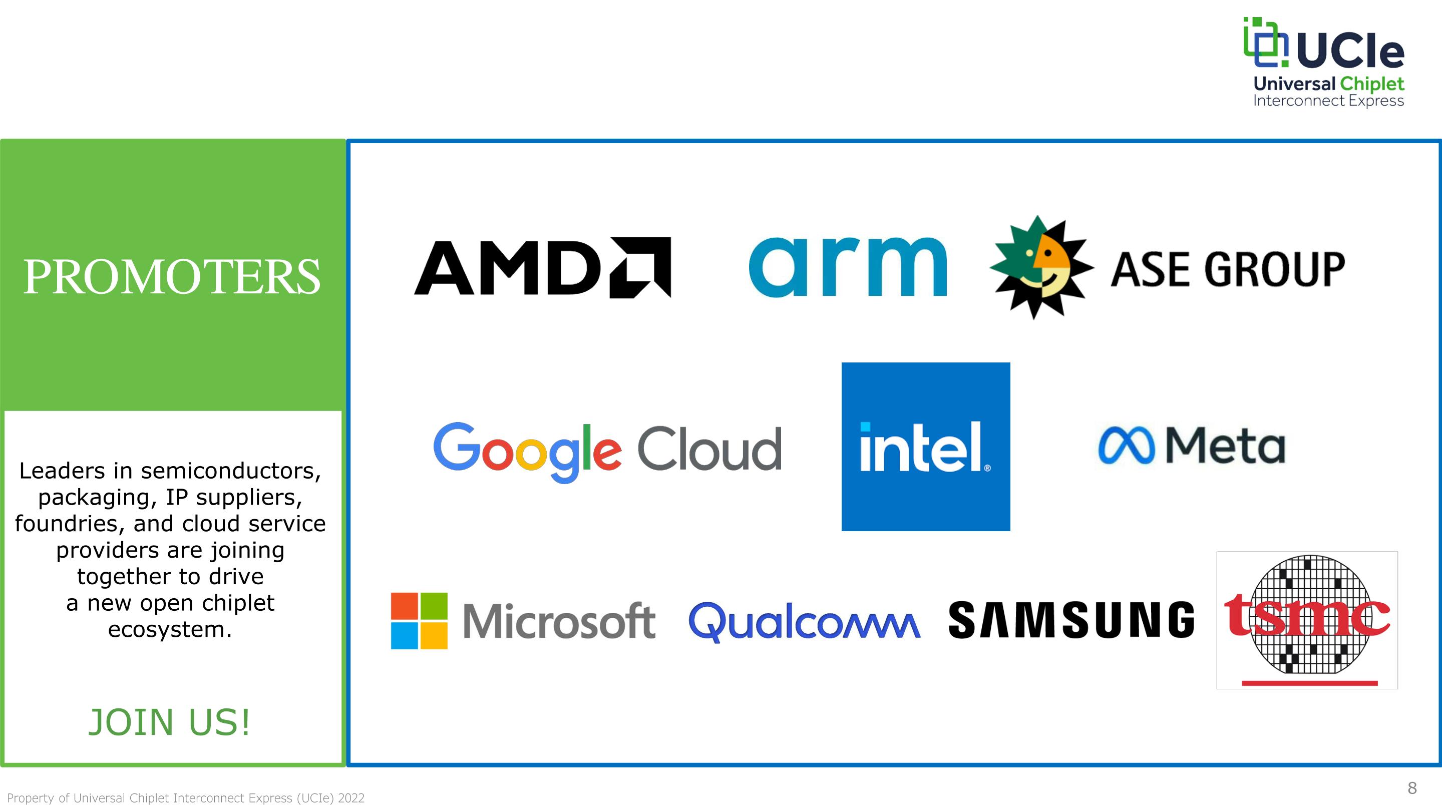
But for that, UCIe will need a proper consortium behind it, which is why today’s announcement is as much a revelation of the new standard as it is a pitch to other companies to join up and help develop future iterations of the standard. The UCIe promoters group is already a very sizable list, featuring backing from chip/IP designers AMD, Arm, Intel, and Qualcomm, chip fabs TSMC and Samsung (and Intel), chip packaging firm Advanced Semiconductor Engineering, and cloud computing providers Google, Microsoft, and Meta.
In short, it’s a who’s who of many of the big players in the chip industry (be them producers or consumers), but the promoters are looking for more members. Pragmatically, the more buy-in the standard gets the more effective and widely adopted it will be, but the group also benefits from the opinions of additional firms, and understanding what their compute needs are.
Full details on the UCIe specification can be found on the group’s new website, including the UCIe whitepaper. Meanwhile interested companies can also find more information on how to join the group as the formal consortium gets created a bit later this year.


25 Comments
View All Comments
dotjaz - Sunday, March 6, 2022 - link
And oh, how exactly do you ban somebody in fear of non-payment when it's free?Oh oh, one more thing, since it happened 7 years ago, and you might not remember. AMD is using MediaTek wireless chips in their platform, pretty impressive considering MTK has no R&D and AMD had to rely on them, wouldn't you imagine AMD had some R&D?
https://www.anandtech.com/show/16666amd-wifi-6e-rz...
dotjaz - Sunday, March 6, 2022 - link
Sorry, replied to the wrong level. Should have been the idiot racist.timecop1818 - Wednesday, March 9, 2022 - link
mediatek GPS has always been dogshit compared to literally every other gps chipset. ublox is vastly superior.dotjaz - Sunday, March 6, 2022 - link
You might be too stupid and racist to comment. MediaTek has their own modem, codec, NPU etc. They are currently the only company using Mali G610/710. And they have been using every Cortex A series within months of launching, barely a quarter behind Qualcomm and Samsung.dotjaz - Sunday, March 6, 2022 - link
Dimensity 9000 was launched merely weeks after Exynos 2200 and barely 2 months after Snapdragon 8 Gen1. I assume your lifespan is about 2500 days, so 30 days might be a "year" for you.eastcoast_pete - Thursday, March 3, 2022 - link
I had the same question. But, many of these current non-participants might well avail themselves of the tech that's outlined in UCIe. Several (such as Apple or NVIDIA) can access the technology through their foundry partners, especially TSMC and Samsung.Pelle Hermanni - Thursday, March 3, 2022 - link
Mediatek is Taiwanese like TSMC, not Chinesebrucethemoose - Wednesday, March 2, 2022 - link
Also, I see "MEMORY" is one of the blocks in those slides... would this standard be used for memory too?Maybe it will be conflated with a future HBM standard?
I can also envision CPUs with low-latency, low power dram sitting right on the (traditional) package, which I would gladly trade off for the expandability of DIMMs.
Wereweeb - Wednesday, March 2, 2022 - link
HBM is just a chiplet, so there's a possibility. And HBM has comparable latency to standard DIMM's. I'd much rather have OMI DIMMs, for more flexibility.Don't forget that silicon devices will have ever increasing failure rates as we shrink them to sizes where the position of one atom makes a difference. Losing modularity for marginal power gains just isn't worth it IMO.
brucethemoose - Wednesday, March 2, 2022 - link
Depends on the gains and the form factor.In a CPU, every bit of memory latency you can shave off is huge... though I'm kinda surprised HBM latency isn't lower than GDDR or DIMMs. Maybe its just not tuned for that?
And in stuff like laptops or consoles, you don't get much modularity anyway, and the saved space on the PCB is a bigger benefit.