AMD's 12-core "Magny-Cours" Opteron 6174 vs. Intel's 6-core Xeon
by Johan De Gelas on March 29, 2010 12:00 AM EST- Posted in
- IT Computing
Magny-Cours
You probably heard by now that the new Opteron 6100 is in fact two 6-core Istanbul CPUs bolted together. That is not too far from the truth if you look at the micro architecture: little has changed inside the core. It is the “uncore” that has changed significantly: the memory controller now supports DDR-1333, and a lot of time has been invested in keeping cache coherency traffic under control. The 1944-pin (!) organic Land Grid Array (LGA) Multi Chip Module (MCM) is pictured below.
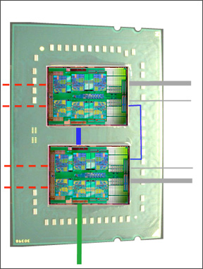
The red lines are memory channels, blue lines internal HT cache coherent connects. The gray lines are external cache HT connections, while the green line is a simple non coherent I/O HT connect.
Each CPU has two DDR-3 channels (red lines). That is exactly the strongest point of this MCM: four fast memory channels that can use DDR-1333, good for a theoretical bandwidth peak of 42.7 GB/s. But that kind of bandwidth is not attainable, not even in theory bBecause the next link in the chain, the Northbridge, only runs at 1.8GHz. We have two 64-bit Northbridges both working at 1.8 GHz, limiting the maximum bandwidth to 28.8 GB/s. That is price AMD’s engineers had to pay to keep the maximum power consumption of a 45nm 2.2 GHz below 115W (TDP).
Adding more cores makes the amount of snoop traffic explode, which can easily result in very poor scaling. It can get worse to the point where extra cores reduce performance. The key technology is HT assist, which we described here. By eliminating unnecessary probes, local memory latency is significantly reduced and bandwidth is saved. It cost Magny-cours 1MB of L3-cache per core (2MB total), but the amount of bandwidth increases by 100% (!) and the latency is reduced to 60% of it would be without HT-assist.
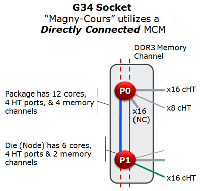
Even with HT-assist, a lot of probe activity is going on. As HT-assist allows the cores to perform directed snoops, it is good to reach each core quickly. Ideally each Magny-cours MCM would have six HT3 ports. One for I/O with a chipset, 2 per CPU node to communicate with the nodes that are off-package and 2 to communicate very quickly between the CPU nodes inside the package. But at 1944 pins Magny-Cours probably already blew the pin budget, so AMD's engineers limited themselves to 4 HT links.
One of the links is reserved for non coherent communication with a possible x16 GPU. One x16 coherent port communicates with the CPU that is the closest, but not on the same package. One port is split in two x8 ports. The first x8 port communicates with the CPU that is the farthest away: for example between CPU node 0 and CPU node 3. The remaing x16 and x8 port are used to make communication on the MCM as fast as possible. Those 24 links connect the two CPU nodes on the package.
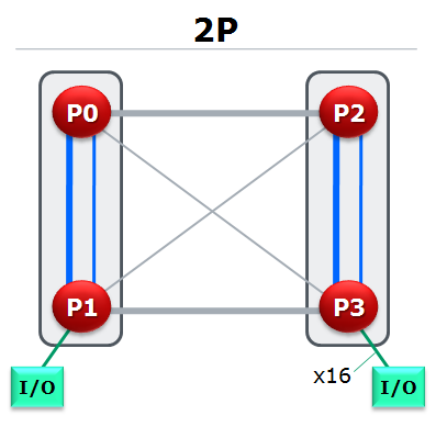
The end result is that a 2P configuration allows fast communication between the four CPU nodes. Each CPU node is connected directly (one hop) with the other one. Bandwidth between CPU node 0 and 2 is twice than that of P0 to P3 however.
Whilte it looks like two Istanbuls bolted together, what we're looking at is the hard work of AMD's engineers. They invested quite a bit of time to make sure that this 12 piston muscle car does not spin it’s wheels all the time. Of course if the underground is wet (badly threaded software), that will still be the case. And that'll be the end of our car analogies...we promise :)


58 Comments
View All Comments
Cogman - Tuesday, March 30, 2010 - link
It should be noted that newer nehelam based processors have specific AES encryption instructions. The benchmark where the xeon blows everything out of the water is likely utilizing that instruction set (though, AFAIK not many real-world applications do)Hector1 - Tuesday, March 30, 2010 - link
I read that Intel is expected to launch the 8-core Nehalem EX today. It'll be interesting to compare it against the 12-core Magny Cours. Both are on a 45nm process.spoman - Tuesday, March 30, 2010 - link
You stated "... that kind of bandwidth is not attainable, not even in theory because the next link in the chain, the Northbridge ...".How does the Northbridge affect memory BW if the memory is connected directly to the processor?
JohanAnandtech - Wednesday, March 31, 2010 - link
Depending on your definition, the nortbridge is in the CPU. AMD uses "northbride" in its own slides to refer to the part where the memory controller etc. resides.Pari_Rajaram - Tuesday, March 30, 2010 - link
Why don't you add STREAM and LINPACK to your benchmark suites? These are very important benchmarks for HPC.JohanAnandtech - Wednesday, March 31, 2010 - link
Stream... in the review.piooreq - Wednesday, March 31, 2010 - link
Hi Johan,For last few days I did several tests with Swingbench CC with similar database configuration but I achieved a bit different results, I’m just wondering what exactly settings you put for CC test itself. I mean about when you generate schema and data for that test? Thanks for answer.
JohanAnandtech - Thursday, April 1, 2010 - link
Your question is not completely clear to me. What is the info you would like? You can e-mail if you like at johanATthiswebsitePointcomzarjad - Wednesday, March 31, 2010 - link
Can't figure out if hyperthreading were enabled on Intels. Particularly interested in virtualization benchmark with hyperthreading both enabled and disabled. Also of interest would be an Office benchmark with a bunch of small VMs (1.5 to 2GB) to simulate VDI configuration.JohanAnandtech - Thursday, April 1, 2010 - link
Hyperthreading is always on. But we will follow up on that. A VDI based hypervisor tests is however not immediately on the horizon. The people of the VRC project might do that though. Google on the VRC project.