AMD and GlobalFoundries, CES 2011
by Jarred Walton on January 7, 2011 3:30 AM ESTGlobalFoundries – Expanding to Meet Demand
It’s been about a year since we last had a serious discussion with GlobalFoundries. Last CES, they were relatively recently separated from AMD and we didn’t have a whole lot to report; 12 months later, there’s a lot more going on. They are now doing full production of 45nm and 40nm chips, the latter going into many of the other electronics devices we use on a regular basis. Where AMD and Intel have lived on the 65nm, 45nm, and now 32nm nodes, most of the other IP developments are happening on the so-called half-nodes. Smartphones and their related technologies are the big one, and GF is working with many of the major players—Qualcomm, ST, ARM, and others. GlobalFoundries now has 300mm fabs in Germany, New York, and Singapore with additional 200mm fabs in Singapore; all told there are 12 locations with approximately 10,000 employees.
One of the big questions last year was how GlobalFoundries would handle the needs of other fabless semiconductor companies. The acquisition of Chartered Semiconductor increased their presence in a big way, also giving GF fabrication facilities in Singapore. While AMD continues to use nearly all of the 45nm capacity, the 40nm production has a long list of partners. The Dresden fab 1 is adding capacity and they’re pushing up to 80,000 wafers per month. The upstate New York fab 8 construction continues to progress, and demand for their services is great enough that GF has already begun working to expand the facility before the current construction is even complete! Fab 8 should come online in 2013, with production focused on 22/20nm output and capacity for around 60,000 wafers per month.
Right now, GlobalFoundries is entering full production mode for 32nm, with AMD’s Llano chips scheduled to be the first market solution to use the process. Later this year, AMD will also launch their Bulldozer cores on the 32nm process. In a similar vein, the 28nm node uses the same gate stack and will leverage the learning of their x86/32nm ramp. Qualification and production of 28nm will continue over the coming year, with plenty of new 28nm devices to come. One of the interesting points GF brought up is that in the past, doing test SRAM wafers has been the common practice for ironing out the glitches in a new process. SRAM wafers produce regular grids where errors are easy to detect; the problem is that complex logic stresses the latest process technology in a different way. To further help with process refinements, GF also runs a test SoC ARM Cortex A9 microprocessor design through the pipeline. The results of this test wafer not only help them find and fix problems, but they also give a better idea of how chips on the new process perform. The following slide summarizes what they’ve seen so far.
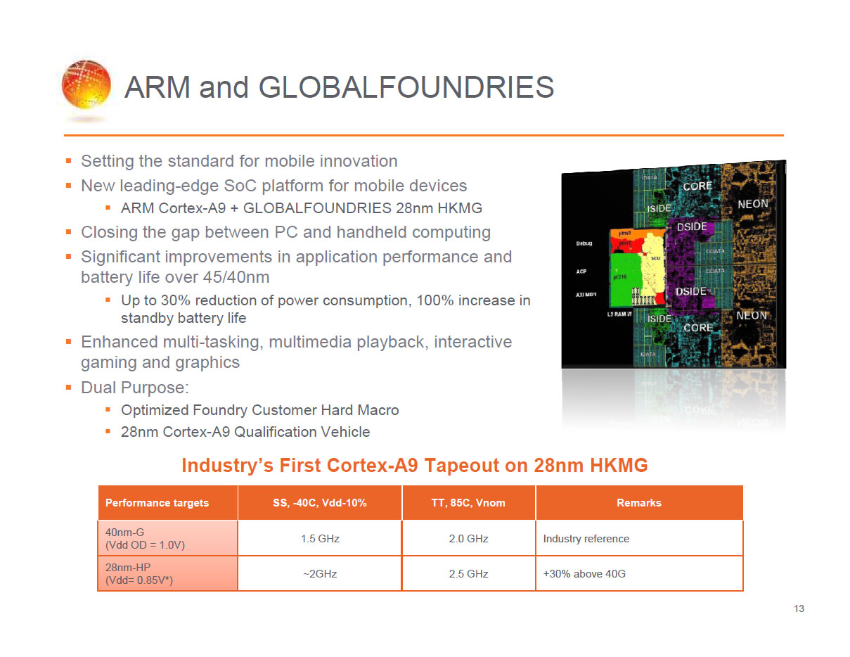
Bumping typical clock speeds from 1.5 to 2.0GHz for the lower power designs, and from 2.0 to 2.5GHz on higher performance chips is good, but even more importantly GF saw power requirements drop up to 30%. Providing 25-33% more performance using 30% less power (and a 100% increase in standby battery life) will be key to enabling the next generation of mobile devices, and we should continue to see a roughly two-fold improvement in performance at a given power envelope every couple of years. Over the course of the year we should see a major transition from 45nm to 32nm for AMD solutions, while the other devices should experience a similar transition from 40nm to 28nm.


GF looks to be doing well, and they are looking like a viable alternative to TSMC for companies looking for fabrication facilities. They have technologies ready for all the electronics segments, from CPUs and microprocessors to smartphones and DTV. They’re also looking at opportunities in the MEMS (Micro Electro Mechanical Systems, i.e. DLP, optical switches) and 3D stacking. Over the next two years, they should more than double their 300mm wafer capacity, and continue R&D into future technologies.
Moving beyond 32nm and 28nm, GlobalFoundries is well into the research and design phase on their 22nm and 20nm nodes. We asked about plans beyond 20nm, and GF says that the current planar transistor commonly used in today’s microprocessors should still be good for a few years. After that, they expect the next five or so generations of process refinements to move to more of a vertical arrangement for the transistor layout. Every so often the naysayers inevitably rear up and claim we’re reaching the end of what we can achieve with semiconductor technology. First it was getting below 1 micron, but we’ve long since smashed that barrier and are moving steadily towards the 1nm mark. How small can we go? No one is willing to call it quits yet at GF, and we expect to see additional creative solutions as we run into technological hurdles.


72 Comments
View All Comments
Edgar_Wibeau - Friday, January 7, 2011 - link
The original plan at the begnning of 2010 was:- Llano first
- Ontario second
- Bulldozer third
Then, further problems emerged with Llano, yiel problems according to AMD, some suspect problems with the GPU-part having yield-problems in 32nm SOI/HKMG which is a completely new process tech for a GPU.
So on the analyst CC in november (even befor that IIRC) the current (inofficial) plan was communicated:
- Ontario first
- Bulldozer starting from april
- Llano in Q3
Some sources now claim a re-push forward to june for Llano, but that's very uncertain as of now.
There are more mistakes in the article, like Ontario is claimed to be manufactured on a 32nm process, which (ULP Bulk CMOS) doesn't even exist neither at TSMC, nor at GloFo. Bothe were cancelled in favour of 28nm.
Maybe Anand should hire an AMD spinner for a change.
http://www.techeye.net/chips/top-intel-spinner-tip...
Edgar_Wibeau - Friday, January 7, 2011 - link
http://www.planet3dnow.de/photoplog/index.php?n=12...Edgar_Wibeau - Friday, January 7, 2011 - link
http://www.planet3dnow.de/photoplog/index.php?n=12...Inofficial of course, could be fakes of course.
spigzone - Friday, January 7, 2011 - link
Charlie said in an article a couple weeks ago on Semiaccurate GloFo's latest Llano respin suddenly came up roses, apparently everything fell into place and they suddenly had a production ready yield. May have resulted in Llano being bumped up ahead of bulldozer.JarredWalton - Friday, January 7, 2011 - link
Okay, so after meeting with AMD yet again today I asked for clarification. Sorry for the misinformation above, but Bulldozer and Llano are both supposed to come out Q2 apparently. I was told they should launch within ~1 month of each other.sirmo - Friday, January 7, 2011 - link
Those are good news. Thanks for the clarification.GeorgeH - Friday, January 7, 2011 - link
"First it was getting below 1 micron, but we’ve long since smashed that barrier and are moving steadily towards the 1nm mark. How small can we go?"Well, the radius of a single atom is ~0.1nm (depending on how you define radius.) I'd say that's a pretty solid floor on feature size. :)
HibyPrime1 - Friday, January 7, 2011 - link
Then they need to get working on making individual electrons into transistors.marraco - Friday, January 7, 2011 - link
No. Miniaturization is dead end.After 1nm we are into picometer scale, on which quantum forces completely changes the rules.
The answer are polinary transistors, which tap picometer capabilities by working with many atoms in coordination, instead to just reducing the number of atoms on the same transistor.
We need to use the same atoms on different transistors, and simultaneously. That way we would increase [logical] transistor density witouth [non-existent] smaller atoms, or stacking layers in 3D.
marraco - Friday, January 7, 2011 - link
Here is the first polinary transistor:http://www.physorg.com/news/2010-10-triple-mode-tr...
It is capable of switch between 3 states instead of the 2 states traditional transistors.
Once we achieve the four states transistor, it will be able to do the work of 2 transistors on the space of one, efectively duplicating density. It is the future of Moore's law, but it requires deeper understanding of quantum forces.