AMD Announces Their First 8000M GPUs
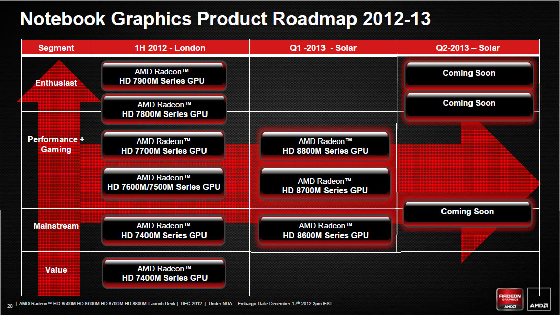
by Jarred Walton on December 17, 2012 4:21 PM ESTAMD held a press briefing today on their upcoming 8000M graphics chips, which they are calling the "second generation GCN architecture" parts. We’ll have more on that in a moment, but while we were expecting (dreading) a rebranding prior to the call, it appears we are at least partially mistaken; there will be at least one completely new GPU with 8000M. (If you want additional background material, you can see the previous generation high-end 7000M announcement from April 2012 for reference.)
I’m not going to get too far into the marketing aspects, as we’ve heard all of this information before: AMD has improved Enduro Technology, they’re continuing to improve their drivers, and APP Acceleration has a few more applications. There have been a few major titles released in the past couple of months with AMD Gaming Evolved branding (Far Cry 3 is arguably the most notable of the offerings, with Hitman: Absolution and Sleeping Dogs also scoring well amongst critics and users), and Bioshock Infinite is at least one future release that I'm looking forward to playing.
Cutting straight to the chase, at this point AMD has released limited information on the core specifications for some of their 8000M GPUs, but they coyly note that at least one more GPU announcement will be forthcoming in Q2 2013 (8900M by all appearances). Today is a soft launch of high level details, with more architectural information and product details scheduled for January 7, 2013 at CES. AMD did not share any codenames for the newly announced mobile GPUs, if you’re wondering, other than the overall family name of “Solar” for the mobile chips (replacing the outgoing “London” series), but we do know from other sources that the 384 core part is codenamed "Mars" while the larger 640 core part is codenamed "Neptune". Here are the details we have right now:
| AMD Radeon HD 8500M, 8600M, 8700M, and 8800M | ||||
|
Radeon HD 8500M |
Radeon HD 8600M |
Radeon HD 8700M |
Radeon HD 8800M |
|
| Stream Processors | 384 | 384 | 384 | 640 |
| Engine Clock | 650MHz | 775MHz | 650-850MHz | 650-700MHz |
| Memory Clock | 2.0GHz/4.5GHz | 2.0GHz/4.5GHz | 2.0GHz/4.5GHz | 4.5GHz |
| Memory Type | DDR3/GDDR5 | DDR3/GDDR5 | DDR3/GDDR5 | GDDR5 |
| FP32 GFLOPS | 537 | 633 | 537-691 | 992 |
| FP64 GFLOPS | 33 | 39 | 33-42 | 62 |
Obviously there are a lot of missing pieces right now, but what we immediately notice is that the core count on the 8500M/8600M/8700M means that we’re definitely looking at a new GPU. The only other time we’ve seen AMD do 384 cores is with Trinity, but that’s a VLIW4 architecture so we’re not seeing that again. Given the currently shipping Southern Islands chips (“London” on the mobile side) have 640 cores max for Cape Verde, 1280 max for Pitcairn, and up to 2048 for Tahiti, AMD has likely created a fourth SI derivative that drops down to two CU arrays, each with three CUs. (You can read more about the GCN/SI architecture in our earlier GPU coverage.) Performance is something of a wildcard with the new 384 core parts, and the choice of DDR3/GDDR5 memory will also influence the final result. We'll find out in the coming months how the 8500/8600/8700M stack up to NVIDIA's midrange "GT" offerings, which interestingly are also using 384 cores.
Also worth a quick note is that AMD is not discussing TDPs at this point in time—which is common practice for both AMD and NVIDIA. We expect the new "Mars" parts to be more power efficient than the outgoing Thames/Turks cores, thanks to the shrink to a 28nm process. However, AMD and NVIDIA typically stick to common power targets for laptops that are dictated by their OEM partners, which often means they'll play with clock speeds in order to hit a specific TDP. That's why all of the clock speeds listed in the above table have a qualifying "up to" prefix (which I omitted).
The final announced card is the one where we appear to have more of a rebrand/optimization of a previous generation chip. 8800M has the same 640 core count as Cape Verde/7800M, only with modified clocks this time. The earlier 7800M chips could clock up as high as 800MHz, so maximum core clock is actually down a bit, but they only ran the memory at up to 1GHz (4GHz effective) GDDR5. If AMD determined memory bandwidth was more important for that particular GPU than shader performance, the new 8800M would make sense. Also note that AMD isn’t including the boost clock speeds into the above chart; under the right circumstances, all of the new chips can run at higher clocks than the reference clock.
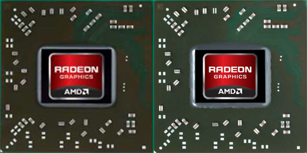
Radeon 7800M Left, Radeon 8800M Right
AMD isn’t calling the 8800M a rebrand, but we’re looking at the same core counts as Cape Verde and the same 28nm process technology, so we wouldn’t expect a substantial change in performance. There’s also the above chip shot as a point of reference. If the 8800M is substantially different from Cape Verde then the above images provided in AMD’s slides must be incorrect, as the new and old chips look the same. Minor tweaks to power use, caching, or other elements notwithstanding, we’re probably dealing with a die respin at most. But, there’s nothing inherently wrong with rebranding—AMD and NVIDIA have both been doing it for some time now. Don’t expect every “upgraded” GPU to be better; a 7400M isn’t faster than a 6700M, and likewise we expect 7700M and 7800M to be faster options than the 384 core 8500M/8600M/8700M and competitive with 8800M. Here’s a quick recap of the same core specs as above for the current 7700M/7800M parts:
| AMD Radeon HD 7700M/7800M Specifications | |||||
|
Radeon HD 7730M |
Radeon HD 7750M |
Radeon HD 7770M |
Radeon HD 7850M |
Radeon HD 7870M |
|
| Stream Processors | 512 | 512 | 512 | 640 | 640 |
| Engine Clock | 575-675MHz | 575MHz | 675MHz | 675MHz | 800MHz |
| Memory Clock | 1.8GHz | 4.0GHz | 4.0GHz | 4.0GHz | 4.0GHz |
| Memory Type | DDR3 | GDDR5 | GDDR5 | GDDR5 | GDDR5 |
| FP32 GFLOPS | 589-691 | 589 | 691 | 864 | 1024 |
| FP64 GFLOPS | 36.8-43.2 | 36.8 | 43.2 | 54 | 64 |
I’ll refrain from commenting too much more about performance of an unreleased part, but AMD indicated their 8870M should be substantially faster than NVIDIA’s current GT 650M GDDR5 (which isn’t too surprising considering clocks and core counts), and the 8770M should likewise be a healthy 20%+ bump in performance relative to the 7670M. I’d rather see comparisons with GTX 670MX and HD 7770M, respectively, but I suspect those wouldn’t be quite as impressive. Anyway, you can see AMD’s comparison charts in the complete slide deck gallery below. Availability of the new GPUs is slated for Q1 2013.


88 Comments
View All Comments
JarredWalton - Tuesday, December 18, 2012 - link
Last time I tried Linux, I actually found it felt every bit as resource intensive as Windows 7. It also took longer to boot and delivered worse battery life. If you're running a stripped down flavor of Linux, as opposed to Ubuntu, I'm sure it can boot more quickly, but part of what makes a modern OS desirable is also what makes it resource intensive.As for performance being better in games, I doubt it -- the GPU is usually the big bottleneck, and the best way to improve GPU utilization is through optimizing the drivers. AMD and NVIDIA have been doing Windows drivers for years with every last ounce of effort put into improving performance; there's no reason to suppose that they would somehow get better results from their Linux drivers.
Open source Linux drivers would be a different matter, but I expect it will take years for the Open Source community to match what AMD has done in terms of optimizations -- unless AMD truly were to release every piece of low level information on their hardware that's necessary in order to properly optimize performance, which isn't going to happen.
CadentOrange - Wednesday, December 19, 2012 - link
I guess YMMV. My laptop gets about 3 hours 30 minutes of battery life under Ubuntu 12.04 while it does only 3 hours under Windows 7. I've no comment about gaming performance as there aren't any games worth playing on Linux until Steam arrives.I am using the closed source AMD Catalyst drivers as the open source drivers do not appear to support power management, so it eats through battery power like it's going out of style.
tuxRoller - Saturday, December 29, 2012 - link
Phoronix tends to get pretty similar benchmarks to windows when using the nvidia blob. I don't think I need to explain why that is to you.CeriseCogburn - Wednesday, December 19, 2012 - link
I think you might want to wait for the massive 100% totally paper launch to "proceed to the era where hardware is actually available secretly to the reviewing e-reporters, before declaring a pure linux support win....You know ?
Like maybe some actual hardware in someone's lab before launching the great celebration of amd keeping it's word....
LOL
Best joke yet, amd keeping it's word.
tipoo - Monday, December 17, 2012 - link
Why can't the series names be consistent across desktop and mobile? You think 7000 series, and you think GCN architecture, but really the mobile parts are on the previous one. And then you hear 8000 series and you think the next architecture, but really they're just finally moving the mobile parts to GCN. Why? What knucklehead thought this was a good idea?tipoo - Monday, December 17, 2012 - link
*Barring the parts noted at the top of the article. But that makes it even more confusing, within the same broad family there are different architectures.JarredWalton - Monday, December 17, 2012 - link
7700M, 7800M, and 7900M are all GCN, but yes, it's a bit of a pain. The reality is that making a new architecture and then executing that across all market segments is very difficult. NVIDIA's solution with 600M was to only do two chips initially, GK107 and GK104 -- and even then they still had a few Fermi-based 600M parts. Considering Cape Verde is totally design complete and needs no further work to ship parts, what would be the incentive to design a replacement that doesn't substantially change performance or features? They did make a replacement for the lower-tier 7500M/7600M, and maybe we'll see 8400M get "retired" -- the 7400M is really not much better than Intel's HD 4000 -- so now everything likely to be used is on 28nm GCN.I'm still curious to see what AMD (and NVIDIA) have planned for their next generation GPUs on desktops. CI (Sea Islands) might improve efficiency in a few areas, but the only way to really make it faster while staying on 28nm is to go bigger, and Tahiti is already plenty big. NVIDIA will no doubt have GK110 based high-end parts, but I'm not sure any of that will touch the mobile market. I suspect we'll be waiting until the next process node before AMD and NVIDIA really get a major generational improvement-- so we're experiencing something similar to how the GeForce 400 and 500 parts weren't all that different, or Radeon 5000/6000.
RussianSensation - Monday, December 17, 2012 - link
I still think it's unacceptable from a marketing point of view to launch an HD8870M part that happens to be slower than HD7870M. That's going to be extremely confusing/unfair to the consumers who don't follow the GPU industry as we do. That is worse than rebadging. That's similar to how HD6850/6870 replaced HD5850/5870 but unless you followed the GPUs closely, you might have thought they were actually superior parts.I think AMD should have just gotten rid of the extra transistors used for double precision compute performance for HD8900 series to make room for more graphical functional units. They could always reintroduce the double precision performance back on 20nm node once transistor space/power consumption permits this. NV's strategy of focusing on lean gaming chips with Kepler paid off and knowing that AMD was going to deal with 28nm node again in 2013, as you said it's hard to imagine how they can squeeze a lot more performance than 15-20% (GTX400 --> 500 or HD5870 --> HD6970 series) without running into die space/power consumption constraints.
silverblue - Monday, December 17, 2012 - link
I'm a bit confused here. Both the 7700 to 7900 ranges for desktop and mobile were GCN with the lower parts VLIW5. As most of the complaints about AMD's rebranding seem to be targeted at their mobile parts, I find this baffling especially considering NVIDIA's attempts at confuddling everybody with the GT 640.Allegedly, Sea Islands breaks the 5B transistor and 32 ROP barriers, but until AMD confirms anything, that's just heresay.
CeriseCogburn - Wednesday, December 19, 2012 - link
Here, be less confused - amd has HACKED their prior core into a tiny bit, and claimed it is releasing a new gpu...*"SI chips (“London” ) have 640 cores max for Cape Verde, 1280 max for Pitcairn, and 2048 for Tahiti...
AMD has likely created a fourth SI derivative that drops down to two CU arrays, each with three CUs. (You can read more about the GCN/SI architecture in our earlier GPU coverage.) "
Oh, in other words, we've seen this chip before, and the prior derivatives are fuller chips and faster. Good job amd, cut your garbage in half or thirds or quarters or one sixth, and "release a new 8000 screamer !"
Not so confusing when the truth is told flat out. I guess amd had some serious binning issues with massive chip failures, so they just hacked off a tiny corner of the gpu that still "worked", kinda, and made it a new release...
" Performance is something of a wildcard with the new 384 core parts, and the choice of DDR3/GDDR5 memory "
Love that, the in cahoots vendors can release the new "screamer 8000 series!" and dump on you with ddr3 for the gpu and NEVER TELL YOU.
Then, as a sick amd penny pinching bankruptcy producing fanatic, you get your ddr3 1/6th the former core piece of crap, and you "sing the praises of your immensely brilliant master builder amd!"
That's going to be another wonderful amd fanboy ride. I guess the lies spewed forth will have to up it another several notches.