Haswell GT3e Pictured, Coming to Desktops (R-SKU) & Notebooks
by Anand Lal Shimpi on April 10, 2013 7:21 PM EST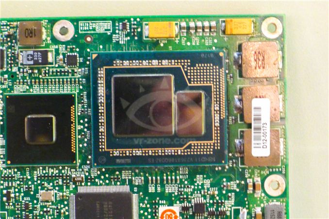
One of the worst kept secrets is Haswell will have four different GPU configurations: GT1, GT2, GT3 and GT3e. As with Sandy Bridge and Ivy Bridge, higher numbers mean more execution units, with GT3 topping out at 40 EUs. The lowercase e denotes an embedded DRAM part, with some amount of DRAM on the Haswell package itself (not on-die).
In an awesome scoop, the folks at VR-Zone managed to snag a photo of what looks like a quad-core Haswell die with GT3e graphics. The small package to the left should be the Lynx Point chipset (8-series), while the dual-die package on the right is Haswell + DRAM. The big square die should be Haswell itself with its 40 EU GPU, while the smaller die is the DRAM itself.
Intel hasn't officially acknowledged the existence of GT3e, but it did demonstrate performance of the part at CES earlier this year - targeting somewhere around the speed of NVIDIA's GeForce GT 650M. The DRAM size, operating frequency and bus width are all unknown at this point. I've heard the DRAM itself should be relatively small (~128MB), looking at the chip shot we get some indication but there's no confirmation of the specific type of memory we're looking at here (which obviously impacts die area).
Haswell GT3e will be available both in notebooks and desktops, however neither will come in socketed form (BGA-only). The desktop parts will carry an R suffix. This will be the beginning of Intel's socketed/soldered strategy on the desktop, which as of now is set to work sort of like tick tock - with the first chips on any new process being sold exclusively in BGA packages. Haswell will have socketed desktop SKUs, Broadwell won't, Skylake will, etc...
GT3e use in notebooks will be limited to larger designs it seems. Don't expect to find this level of graphics performance in a low wattage Ultrabook part, but it will likely surface in bigger notebooks - perhaps those driving ultra high resolution panels.
Source: VR Zone


64 Comments
View All Comments
StevoLincolnite - Friday, April 12, 2013 - link
Those $600 CPU's are indeed faster than the cheaper $300 ones, otherwise there would be NO point in asking $600 for it.In gaming sure, the difference might be negligible, but games are becoming more and more heavily threaded anyway.
microsoftenator - Monday, April 15, 2013 - link
With Intel's CPU sockets the way they are now, you're already upgrading the socket every other generation anyway. This will only really hit the people who upgrade every cycle, ie. enthusiasts who already likely buy the higher-end parts.fteoath64 - Tuesday, April 16, 2013 - link
That unfortunately would be one consequence of socketed MB. I agree that decoupling on low end cpus does not make sense but mid-end to high-end CPUs, there is no gain in cost savings as such. MB tend to go south due to capacitor blowouts and blownouts of some of the resistor circuits so the cpu is 100X more reliable than MB as such. Even corrosion of some joints costs a few MB to go south after some years of use if not cleaned often.UpSpin - Thursday, April 11, 2013 - link
I personally never upgraded the CPU only. I always bought a MB and with it the CPU I liked.After several years I needed a faster PC. But those new CPUs weren't compatible with my old MB any longer, also did new MBs support better RAM/have new ports/features, thus I had and wanted to buy a new MB, too.
A new CPU generation won't be compatible with the old socket any longer, because Intel is heavily changing the CPU/GPU/Chipset model to a SoC, they integrated the power controllers already and so will they integrate other stuff, too, and they have to do it at a very fast speed, else they will be beaten by the ARM based SoCs, because integrating it on a SoC makes it faster, more power efficient, cheaper and smaller.
But because they know that there are some enthusiasts out there which spend all their money on the latest tech and upgrade almost daily to new tech, they'll have to still offer socketed models for those people, too, but they're probably only a minority (most people don't even have a desktop any longer, but an Ultrabook or All-in-one system)
JPForums - Thursday, April 11, 2013 - link
Integrating things onto a SoC does not make them automatically faster, more power efficient, or cheaper. It usually does allow for a smaller overall system, but that is less a concern for PCs and tablets as it is for smart phones (or very small tablets).On die integration does provide for a shorter (lower latency) path, but it is also more space limited which could reduce communications width. In bandwidth limited applications, using a higher bandwidth off die solution could be faster. As an example, a Pentium 4 would most certainly be better off with a dual 64bit channel memory solution than a single (probably 32bit) on die solution as its cache architecture was design to hide memory latency, but a lack of bandwidth would starve the chip.
On die integration can be (and usually is) more power efficient, but it does require redesigning the integrated component to work of the available power plane. You don't really save any power if you bring all of the auxiliary circuitry with it.
On die integration can make a system less expensive, but it can also make it more expensive. On the upside, you remove most of the cost of packaging a separate chip. On the down side, you increase the size (cost) of the chip you are integrating into. Which ends up cheaper is highly dependent on how big the chip is, how much the chip size increases, how mature the fabrication process is, and how big your silicon wafers are. Wafers are roughly fixed in cost, so the cost of individual chips depends directly on how many can be successfully fabricated per wafer. Large chips waste a lot of silicon given that rectangular dies don't match well with circular wafers. Also note that the number of defects on a wafer are not dependent on what is being fabricated. The probability per chip of a critical defect goes up exponentially as die size increases. Redundant resources can be disabled to prevent defects from trashing a chip entirely (think cache or GPU pipelines, unified shaders, etc). However, adding in these resources specifically to disable can be self defeating if the die area (and probability of defect) increases more than the redundant resource compensates. Given a small chip, an increase in size has a greater effect on number of chips per wafer, but does not increase the probability of critical defects nearly as significantly as with larger chips. Fabrication processes with high defect rates favor smaller chips as less silicon per ends up in the garbage. Given a lower defect rate, larger dies may be fabricated with a less significant increase in cost. It makes sense to integrate when the difference in package costs are higher than the difference in silicon costs.
While heavy integration generally leads to smaller overall packages, it can lead to chips with higher thermal densities. This in turn requires better cooling that can eat up the space you saved. This isn't much of a concern with lower power (and hence cooler) chips, but higher performance chips have to take this into account. Thankfully (or rather by design), the smart phone arena that needs smaller is also generally cooler.
The point is, ARM SoCs aren't magically going to get as fast as Intel desktop/laptop chips because they are highly integrated. If that were the case, they would've been there a long time ago. Further, if integration were a magic bullet, ARM would be in trouble as they've already seen the benefits and Intel is still working on it and thus still has benefits to receive. Integration may be a tool to allow ARM to get faster (or Intel to get more power efficient), but it is the Cortex A57/Haswell architectures designed to take advantage of this tool that does most of the work.
UpSpin - Thursday, April 11, 2013 - link
You talk a lot, a lot is right, but some things are wrong or just very near-sighted:Integration makes all I said, and it's more than just being smaller.
Your memory example is correct, but don't forget that I talked about what Intel will do in the future and not how it would have been in the past. They also won't put the memory on the same die, but on top of it, as it's common practice with ARM SoCs. And even NVidia announced to do this in future iterations because of the tremendous benefits. The advantage is not only that it's faster, but also the board design gets simplified.
Power: Sure you have to alter your design, but that's always the case. By integrating the power regulation you can switch faster and more precise, less power gets wasted in the transformation and less external components are required, so the board layout gets simpler, cheaper and smaller.
On die integration will make the particular component more exepensive, but the system cheaper, because you need less external space/parts/engineering. Your argument with the wafer is valid, and probably a difficulty Intel currently has.
Cooling: We don't live in Pentium IV times, which consumed insane amounts of power which made it difficult to cool the CPU. Todays GPUs consume more than any CPU, yet they are still pretty easy and silently to cool. Additionally gets it easier to cool it if everything sits at one place (as long as the overall power consumption remains in current regions). You don't have to use large heatpipes which spread across multiple distant chips, but can focus on cooling a single chip and place that one as close to the cooler as possible and cool this single one as good as possible. On a GPU you have to cool die and mosfets and RAM and guide the air flow properly. The GPU gets cooled properly with a copper core, the RAM often with just some extra alu heatsinks, the mosfets sometimes just with air. If everything is in one place you can focus on a single spot, don't have to save money on bad cooling of external components. The same in notebooks, if you can focus on one part, it gets much easier to keep it cool.
ARM/Intel: I never said that ARM will be faster than Intel just because of integration, I only said that ARM has a huge advantage because they have a much better integration, but I also believe that Intel can tune their efficiency by a much larger degree than ARM can, mainly because of the currently missing integration in Intel designs. On the other hand, ARM is several manufacturing processes behind (28nm vs. 22nm), so they can tune their efficiency that way easily.
Sure, architecture improvements will make the bigger difference, but the other factors contribute a lot to efficiency and speed, too, and only allow some specific architecture changes.
IntelUser2000 - Thursday, April 11, 2013 - link
Sockets are actually supposed to cost few dollars on a motherboard, $3-5 or so. That may actually be quite a bit depending on how much the motherboard costs to make.tipoo - Wednesday, April 10, 2013 - link
I wonder how much power consumption that eDRAM die adds? Would the mobile version be suitable for 13" non-ultrabook laptops?tipoo - Wednesday, April 10, 2013 - link
In theory, someone less lazy than I should be able to figure out the size of that eDRAM package by the measurements of other known features (like the motherboard screw hole for instance), then using that as a reference to get the square area of the eDRAM package. That's what was done when the Wii U GPU was put under a microscope by chipworks, people figured out the size of the eDRAM as well as sRAM on-package.Khato - Wednesday, April 10, 2013 - link
We can get a reasonable guess as to die size, but as stated in the article the actual capacity depends upon both die size and RAM type/process.As for sizes, the one component of reasonable size and 'known' dimensions in the shot are the tantalum surface mount capacitors - they appear to be 6.0x3.2mm for the black and 7.3x4.3mm for the yellow ones. From that we can guess that Intel is continuing to make their ICH a nice square dimension since the pix/mm derived from the capacitors works out to pretty much 20x20mm for the ICH. Lastly that can be used to give us a rough die size estimate of 260mm^2 for the CPU and 80mm^2 for the memory chip. (Probably accurate to within +/- 5% so long as my guess about the ICH dimensions is correct.)