Intel Iris Pro 5200 Graphics Review: Core i7-4950HQ Tested
by Anand Lal Shimpi on June 1, 2013 10:01 AM EST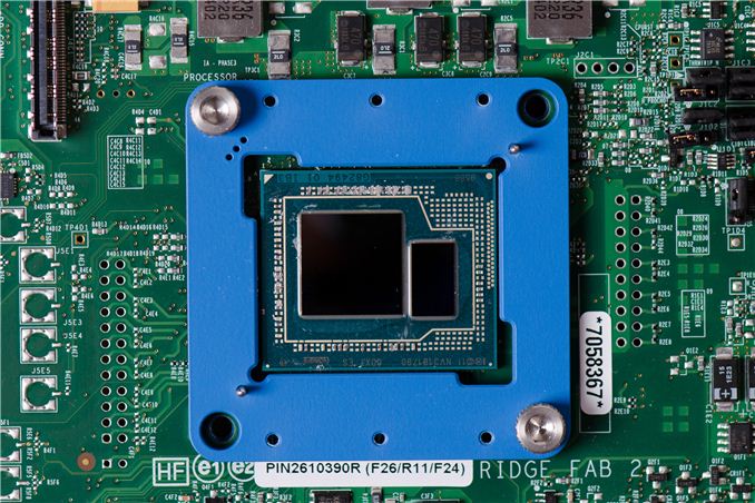
The Prelude
As Intel got into the chipset business it quickly found itself faced with an interesting problem. As the number of supported IO interfaces increased (back then we were talking about things like AGP, FSB), the size of the North Bridge die had to increase in order to accommodate all of the external facing IO. Eventually Intel ended up in a situation where IO dictated a minimum die area for the chipset, but the actual controllers driving that IO didn’t need all of that die area. Intel effectively had some free space on its North Bridge die to do whatever it wanted with. In the late 90s Micron saw this problem and contemplating throwing some L3 cache onto its North Bridges. Intel’s solution was to give graphics away for free.
The budget for Intel graphics was always whatever free space remained once all other necessary controllers in the North Bridge were accounted for. As a result, Intel’s integrated graphics was never particularly good. Intel didn’t care about graphics, it just had some free space on a necessary piece of silicon and decided to do something with it. High performance GPUs need lots of transistors, something Intel would never give its graphics architects - they only got the bare minimum. It also didn’t make sense to focus on things like driver optimizations and image quality. Investing in people and infrastructure to support something you’re giving away for free never made a lot of sense.
Intel hired some very passionate graphics engineers, who always petitioned Intel management to give them more die area to work with, but the answer always came back no. Intel was a pure blooded CPU company, and the GPU industry wasn’t interesting enough at the time. Intel’s GPU leadership needed another approach.
A few years ago they got that break. Once again, it had to do with IO demands on chipset die area. Intel’s chipsets were always built on a n-1 or n-2 process. If Intel was building a 45nm CPU, the chipset would be built on 65nm or 90nm. This waterfall effect allowed Intel to help get more mileage out of its older fabs, which made the accountants at Intel quite happy as those $2 - $3B buildings are painfully useless once obsolete. As the PC industry grew, so did shipments of Intel chipsets. Each Intel CPU sold needed at least one other Intel chip built on a previous generation node. Interface widths as well as the number of IOs required on chipsets continued to increase, driving chipset die areas up once again. This time however, the problem wasn’t as easy to deal with as giving the graphics guys more die area to work with. Looking at demand for Intel chipsets, and the increasing die area, it became clear that one of two things had to happen: Intel would either have to build more fabs on older process nodes to keep up with demand, or Intel would have to integrate parts of the chipset into the CPU.
Not wanting to invest in older fab technology, Intel management green-lit the second option: to move the Graphics and Memory Controller Hub onto the CPU die. All that would remain off-die would be a lightweight IO controller for things like SATA and USB. PCIe, the memory controller, and graphics would all move onto the CPU package, and then eventually share the same die with the CPU cores.
Pure economics and an unwillingness to invest in older fabs made the GPU a first class citizen in Intel silicon terms, but Intel management still didn’t have the motivation to dedicate more die area to the GPU. That encouragement would come externally, from Apple.
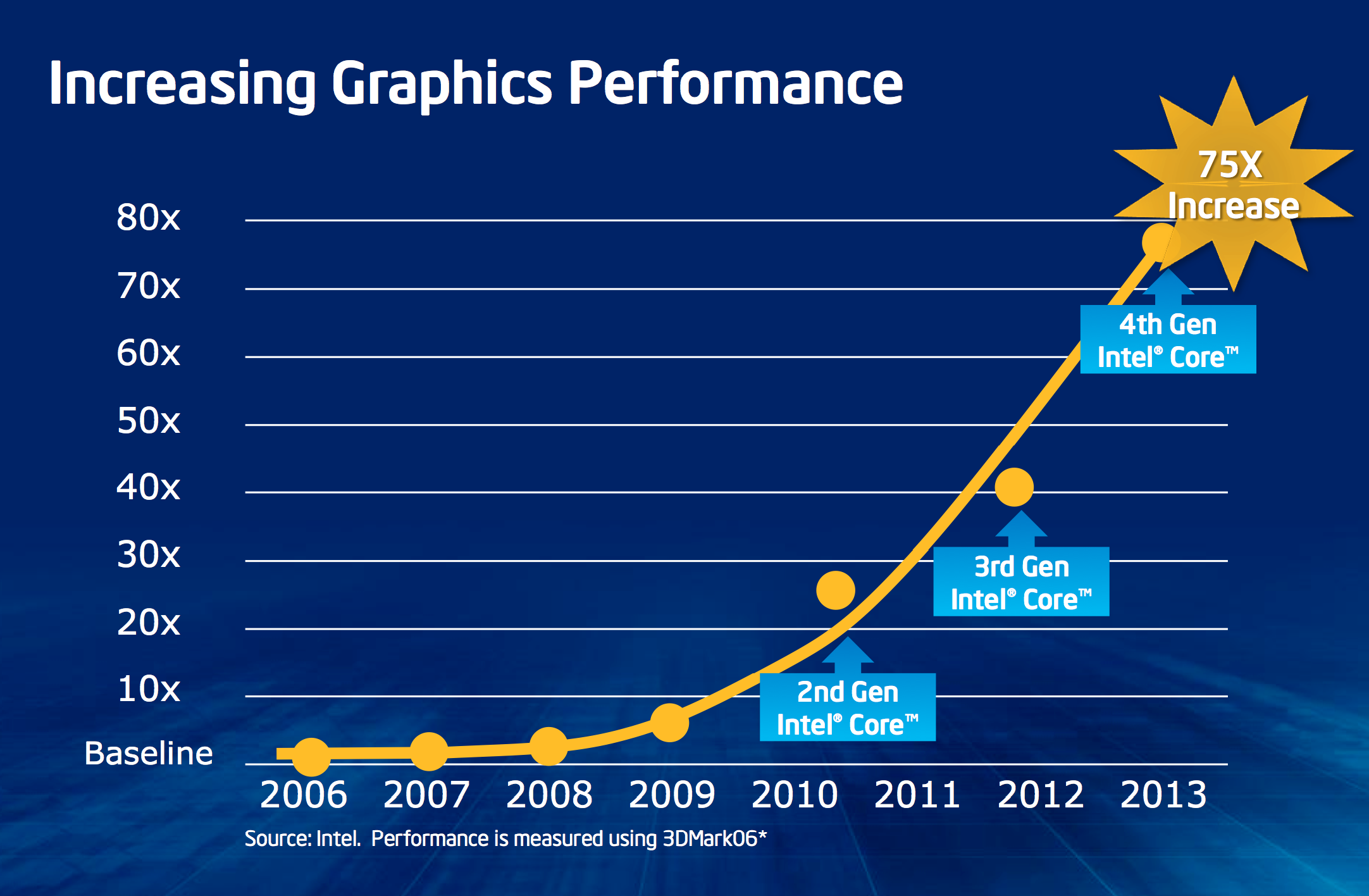
Looking at the past few years of Apple products, you’ll recognize one common thread: Apple as a company values GPU performance. As a small customer of Intel’s, Apple’s GPU desires didn’t really matter, but as Apple grew, so did its influence within Intel. With every microprocessor generation, Intel talks to its major customers and uses their input to help shape the designs. There’s no sense in building silicon that no one wants to buy, so Intel engages its customers and rolls their feedback into silicon. Apple eventually got to the point where it was buying enough high-margin Intel silicon to influence Intel’s roadmap. That’s how we got Intel’s HD 3000. And that’s how we got here.


177 Comments
View All Comments
Elitehacker - Tuesday, September 24, 2013 - link
Even for a given power usage the 650M isn't even to on the top of the list for highest end discrete GPU.... The top at the moment for lowest wattage to power ratio would be the 765M, even the Radeon HD 7750 has less wattage and a tad more power than the 650M. Clearly someone did not do their researching before opening their mouth.I'm gonna go out on a limb and say that vFunct is one of those Apple fanboys that knows nothing about performance. You can get a PC laptop in the same size and have better performance than any Macbook available for $500 less. Hell you can even get a Tablet with an i7 and 640M that'll spec out close to the 650M for less than a Macbook Pro with 650M.
Eric S - Tuesday, June 25, 2013 - link
The Iris Pro 5200 would be ideal for both machines. Pro users would benefit from ECC memory for the GPU. The Iris chip uses ECC memory making it ideal for OpenCL workloads in Adobe CS6 or Final Cut X. Discrete mobile chips may produce errors in the OpenCL output. Gamers would probably prefer a discrete chip, but that isn't the target for these machines.Eric S - Monday, July 1, 2013 - link
I think Apple cares more about the OpenCL performance which is excellent on the Iris. I doubt the 15" will have a discrete GPU. There isn't one fast enough to warrant it over the Iris 5200. If they do ever put a discrete chip back in, I hope they go with ECC GDDR memory. My guess is space savings will be used for more battery. It is also possible they may try to reduce the display bezel.emptythought - Tuesday, October 1, 2013 - link
It's never had the highest end chip, just the best "upper midrange" one. Above the 8600m GT was the 8800m GTX and GTS, and above the 650m there was the 660, a couple 670 versions, the 675 versions, and the 680.They chose the highest performance part that hit a specific TDP, stretching a bit from time to time. It was generally the case that anything which outperformed the MBP was either a thick brick, or had perpetual overheating issues.
CyberJ - Sunday, July 27, 2014 - link
Not even close, but whatever floats you boat.emptythought - Tuesday, October 1, 2013 - link
It wouldn't surprise me if the 15in just had the "beefed up" iris pro honestly. They might even get their own, special even more overclocked than 55w version.Mainly, because it wouldn't be without precedent. Remember when the 2009 15in macbook pro had a 9400m still? Or when they dropped the 320m for the hd3000 even though it was slightly slower?
They sometimes make lateral, or even slightly backwards moves when there are other motives at play.
chipped - Sunday, June 2, 2013 - link
That's just crazy talk, they want drop dedicated graphics. The difference is still too big, plus you can't sell a $2000 laptop without a dedicated GFX.shiznit - Sunday, June 2, 2013 - link
considering Apple specifically asked for eDRAM and since there is no dual core version yet for the 13", I'd say there is very good chance.mavere - Sunday, June 2, 2013 - link
"The difference is still too big"The difference in what?
Something tells me Apple and its core market is more concerned with rendering/compute performance more than Crysis 3 performance...
iSayuSay - Wednesday, June 5, 2013 - link
If it plays Crysis 3 well, it can render/compute/do whatever intensive fine.