AMD Kaveri Docs Reference Quad-Channel Memory Interface, GDDR5 Option
by Anand Lal Shimpi on January 16, 2014 10:51 PM EST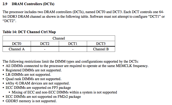
Our own Ryan Smith pointed me at an excellent thread on Beyond3D where forum member yuri ran across a reference to additional memory controllers in AMD's recently released Kaveri APU. AMD's latest BIOS and Kernel Developer's Guide (BKDG 3.00) for Kaveri includes a reference to four DRAM controllers (DCT0 - 3) with only two in use (DCT0 and DCT3). The same guide also references a Gddr5Mode option for each DRAM controller.

Let me be very clear here: there's no chance that the recently launched Kaveri will be capable of GDDR5 or 4 x 64-bit memory operation (Socket-FM2+ pin-out alone would be an obvious limitation), but it's very possible that there were plans for one (or both) of those things in an AMD APU. Memory bandwidth can be a huge limit to scaling processor graphics performance, especially since the GPU has to share its limited bandwidth to main memory with a handful of CPU cores. Intel's workaround with Haswell was to pair it with 128MB of on-package eDRAM. AMD has typically shied away from more exotic solutions, leaving the launched Kaveri looking pretty normal on the memory bandwidth front.
In our Kaveri review, we asked the question whether or not any of you would be interested in a big Kaveri option with 12 - 20 CUs (768 - 1280 SPs) enabled, basically a high-end variant of the Xbox One or PS4 SoC. AMD would need a substantial increase in memory bandwidth to make such a thing feasible, but based on AMD's own docs it looks like that may not be too difficult to get.
There were rumors a while back of Kaveri using GDDR5 on a stick but it looks like nothing ever came of that. The options for a higher end Kaveri APU would have to be:
1) 256-bit wide DDR3 interface with standard DIMM slots, or
2) 256-bit wide GDDR5 interface with memory soldered down on the motherboard
I do wonder if AMD would consider the first option and tossing some high-speed memory on-die (similar to the Xbox One SoC).
All of this is an interesting academic exercise though, which brings me back to our original question from the Kaveri review. If you had the building blocks AMD has (Steamroller cores and GCN CUs) and the potential for a wider memory interface, would you try building a high-end APU for the desktop? If so, what would you build and why?
I know I'd be interested in a 2-module Steamroller core + 20 CUs with a 256-bit wide DDR3 interface, assuming AMD could stick some high-bandwidth memory on-die as well. More or less a high-end version of the Xbox One SoC. Such a thing would interest me but I'm not sure if anyone would buy it. Leave your thoughts in the comments below, I'm sure some important folks will get to read them :)


127 Comments
View All Comments
hodakaracer96 - Thursday, January 16, 2014 - link
Lets say the Kinect cost $100 so both the xbox one and PS4 are the same price. It seems like PS4's gddr5 solution beat the xbox on performance so it is the right way for an APU to go at this time? Or is sony just taking a hit financially? I know there are a lot of variables to cost/performance between the two solutions. Either way, AMD should have the chip for it, probably even more so with the GDDR5 solution. Didn't xbox do a lot of the work themselves on their SOC? I'm more interested lowering overall power under high load for some on the go gaming than a desktop solution.hodakaracer96 - Thursday, January 16, 2014 - link
Or possibly once games are coded to use the on chip memory solution the performance/price gap will decrease.Gabrielsp85 - Thursday, January 16, 2014 - link
X1 CPU is 3 times more efficient than the PS4 CPU, also i don't think Sonys cheap design will top MS after all the money they spent on R&Dchaosbloodterfly - Friday, January 17, 2014 - link
Where the hell did you get that number? They both have the same architecture and process. There's no way to get a 3x efficiency increase while keeping those constant.It also wouldn't matter at all. The PS4 isn't noisy, nor does it run on battery. Not to mention it's all about the GPU.
Gabrielsp85 - Friday, January 17, 2014 - link
16 opc vs 48 opc on X1meacupla - Friday, January 17, 2014 - link
From what I have read..."A Jaguar core can issue 6 ops per cycle -- two memory, two int alu, and two fpu/simd ops. However, it can only decode two, and retire two, so the average rate cannot ever go above two."
Gabrielsp85 - Friday, January 17, 2014 - link
X1 CPU is customized not a "stock" Jaguar. "to get all of this processing out of the box" is a challenge too.The new CPU core can do six CPU operations per core per cycle, on an eight-core CPU." -Nick BakerChilder - Friday, January 17, 2014 - link
From the XOne documentation, i don't see any difference from a regular Jaguar core, it can decode and retire only 2 instructions per cycle. Up to 6 µ-ops at once, 1 load, 1 store, 2 ALU and 2 FPU.Renderer - Friday, January 17, 2014 - link
No one remembers Microsoft saying that it was a custom built CPU apparently.MrSpadge - Friday, January 17, 2014 - link
Of course they would say so. And how many transistors would they need to change (e.g. eDRAM access) to call it custom?