Apple's Cyclone Microarchitecture Detailed
by Anand Lal Shimpi on March 31, 2014 2:10 AM EST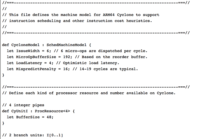
The most challenging part of last year's iPhone 5s review was piecing together details about Apple's A7 without any internal Apple assistance. I had less than a week to turn the review around and limited access to tools (much less time to develop them on my own) to figure out what Apple had done to double CPU performance without scaling frequency. The end result was an (incorrect) assumption that Apple had simply evolved its first ARMv7 architecture (codename: Swift). Based on the limited information I had at the time I assumed Apple simply addressed some low hanging fruit (e.g. memory access latency) in building Cyclone, its first 64-bit ARMv8 core. By the time the iPad Air review rolled around, I had more knowledge of what was underneath the hood:
As far as I can tell, peak issue width of Cyclone is 6 instructions. That’s at least 2x the width of Swift and Krait, and at best more than 3x the width depending on instruction mix. Limitations on co-issuing FP and integer math have also been lifted as you can run up to four integer adds and two FP adds in parallel. You can also perform up to two loads or stores per clock.
With Swift, I had the luxury of Apple committing LLVM changes that not only gave me the code name but also confirmed the size of the machine (3-wide OoO core, 2 ALUs, 1 load/store unit). With Cyclone however, Apple held off on any public commits. Figuring out the codename and its architecture required a lot of digging.
Last week, the same reader who pointed me at the Swift details let me know that Apple revealed Cyclone microarchitectural details in LLVM commits made a few days ago (thanks again R!). Although I empirically verified many of Cyclone's features in advance of the iPad Air review last year, today we have some more concrete information on what Apple's first 64-bit ARMv8 architecture looks like.
Note that everything below is based on Apple's LLVM commits (and confirmed by my own testing where possible).
| Apple Custom CPU Core Comparison | ||||||
| Apple A6 | Apple A7 | |||||
| CPU Codename | Swift | Cyclone | ||||
| ARM ISA | ARMv7-A (32-bit) | ARMv8-A (32/64-bit) | ||||
| Issue Width | 3 micro-ops | 6 micro-ops | ||||
| Reorder Buffer Size | 45 micro-ops | 192 micro-ops | ||||
| Branch Mispredict Penalty | 14 cycles | 16 cycles (14 - 19) | ||||
| Integer ALUs | 2 | 4 | ||||
| Load/Store Units | 1 | 2 | ||||
| Load Latency | 3 cycles | 4 cycles | ||||
| Branch Units | 1 | 2 | ||||
| Indirect Branch Units | 0 | 1 | ||||
| FP/NEON ALUs | ? | 3 | ||||
| L1 Cache | 32KB I$ + 32KB D$ | 64KB I$ + 64KB D$ | ||||
| L2 Cache | 1MB | 1MB | ||||
| L3 Cache | - | 4MB | ||||
As I mentioned in the iPad Air review, Cyclone is a wide machine. It can decode, issue, execute and retire up to 6 instructions/micro-ops per clock. I verified this during my iPad Air review by executing four integer adds and two FP adds in parallel. The same test on Swift actually yields fewer than 3 concurrent operations, likely because of an inability to issue to all integer and FP pipes in parallel. Similar limits exist with Krait.
I also noted an increase in overall machine size in my initial tinkering with Cyclone. Apple's LLVM commits indicate a massive 192 entry reorder buffer (coincidentally the same size as Haswell's ROB). Mispredict penalty goes up slightly compared to Swift, but Apple does present a range of values (14 - 19 cycles). This also happens to be the same range as Sandy Bridge and later Intel Core architectures (including Haswell). Given how much larger Cyclone is, a doubling of L1 cache sizes makes a lot of sense.
On the execution side Cyclone doubles the number of integer ALUs, load/store units and branch units. Cyclone also adds a unit for indirect branches and at least one more FP pipe. Cyclone can sustain three FP operations in parallel (including 3 FP/NEON adds). The third FP/NEON pipe is used for div and sqrt operations, the machine can only execute two FP/NEON muls in parallel.
I also found references to buffer sizes for each unit, which I'm assuming are the number of micro-ops that feed each unit. I don't believe Cyclone has a unified scheduler ahead of all of its execution units and instead has statically partitioned buffers in front of each port. I've put all of this information into the crude diagram below:
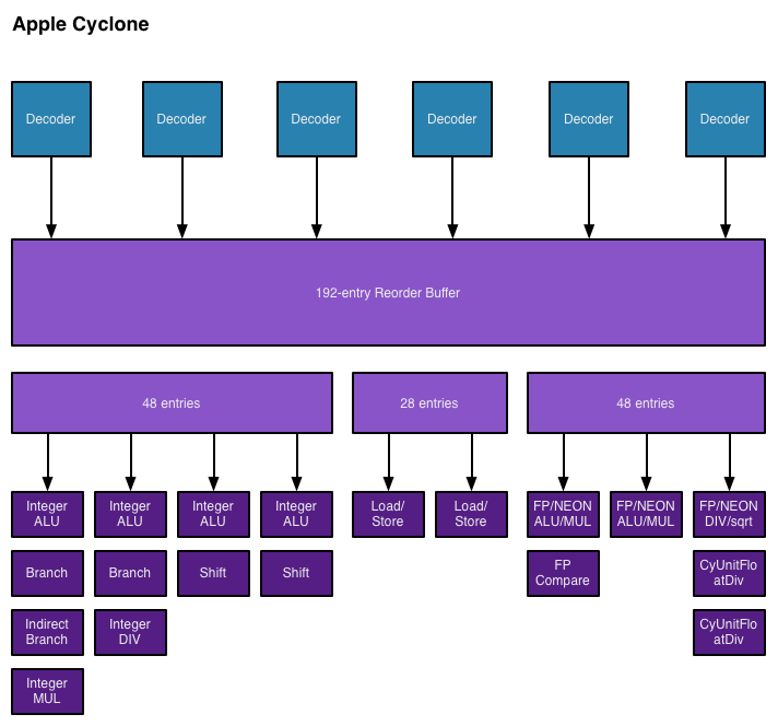
Unfortunately I don't have enough data on Swift to really produce a decent comparison image. With six decoders and nine ports to execution units, Cyclone is big. As I mentioned before, it's bigger than anything else that goes in a phone. Apple didn't build a Krait/Silvermont competitor, it built something much closer to Intel's big cores. At the launch of the iPhone 5s, Apple referred to the A7 as being "desktop class" - it turns out that wasn't an exaggeration.
Cyclone is a bold move by Apple, but not one that is without its challenges. I still find that there are almost no applications on iOS that really take advantage of the CPU power underneath the hood. More than anything Apple needs first party software that really demonstrates what's possible. The challenge is that at full tilt a pair of Cyclone cores can consume quite a bit of power. So for now, Cyclone's performance is really used to exploit race to sleep and get the device into a low power state as quickly as possible. The other problem I see is that although Cyclone is incredibly forward looking, it launched in devices with only 1GB of RAM. It's very likely that you'll run into memory limits before you hit CPU performance limits if you plan on keeping your device for a long time.
It wasn't until I wrote this piece that Apple's codenames started to make sense. Swift was quick, but Cyclone really does stir everything up. The earlier than expected introduction of a consumer 64-bit ARMv8 SoC caught pretty much everyone off guard (e.g. Qualcomm's shift to vanilla ARM cores for more of its product stack).
The real question is where does Apple go from here? By now we know to expect an "A8" branded Apple SoC in the iPhone 6 and iPad Air successors later this year. There's little benefit in going substantially wider than Cyclone, but there's still a ton of room to improve performance. One obvious example would be through frequency scaling. Cyclone is clocked very conservatively (1.3GHz in the 5s/iPad mini with Retina Display and 1.4GHz in the iPad Air), assuming Apple moves to a 20nm process later this year it should be possible to get some performance by increasing clock speed scaling without a power penalty. I suspect Apple has more tricks up its sleeve than that however. Swift and Cyclone were two tocks in a row by Intel's definition, a third in 3 years would be unusual but not impossible (Intel sort of committed to doing the same with Saltwell/Silvermont/Airmont in 2012 - 2014).
Looking at Cyclone makes one thing very clear: the rest of the players in the ultra mobile CPU space didn't aim high enough. I wonder what happens next round.


182 Comments
View All Comments
jasonelmore - Monday, March 31, 2014 - link
I thought intel's SOC's will be produced on the Latest Node? ie: 14nm they made the announcement 1 year ago. 14nm is beginning production in June and shipping August-September (This year) and that's with the delays factored injeffkibuule - Monday, March 31, 2014 - link
Intel's also had FinFET for 1-2 years, whereas TSMC won't roll it out until 16nm? That's still and advantage as well.dylan522p - Monday, March 31, 2014 - link
They are. Airmont is Q3/4. Intel is actually not doing Broadwell for most desktop so they can allocate to to airmont. TSMC won't be able to do 20nm FinFET (which Intel had with ivy a while ago) a die the size of ivy (which is fairly tiny) until late 2015.dylan522p - Monday, March 31, 2014 - link
Umm no they aren't. They are calling 20nm FinFet 16nm. Intel had that over 2 years ago. They used to be a year and half behind and its slipping.raghu78 - Monday, March 31, 2014 - link
sorry but Intel's node naming is misleading. Intel's 22nm FINFET transistor density is comparable to TSMC 28nm. Both use single pattern immersion litho. transistor perf is superior on Intel 22 nm FINFET.Intel 14nm and TSMC 16FF both use dual pattern immersion litho. the M1 metal pitch is 64nm for both these processes. Intel has no significant transistor density advantage over TSMC. TSMC is also developing a improved version of 16FF called 16FF+. That process matches Intel 14nm in performance.
http://electronics360.globalspec.com/article/3974/...
name99 - Monday, March 31, 2014 - link
Intel also has more restrictive design rules than TSMC et al.It is true that Intel got to FinFET first, and good for them. But one can turn that around and say that it's NOT a good sign that Intel's most kickass fabs produce something that is still not competitive in phones with what's produced by everyone else's fab.
Intel MAY have an advantage in materials. That's very much an area of randomness and luck. They seem to take materials research more seriously than their competitors (or at least they did in the past). But it's also possible that we've hit the wall on what we can do with materials (low-K dielectrics, better insulators, copper interconnect etc) beyond a few percent increases --- I don't know enough to have an opinion.
Kidster3001 - Monday, April 7, 2014 - link
You keep believing that.blanarahul - Monday, March 31, 2014 - link
"While TSMC will have its 16nm in 2nd half of 2015."I find this hard to believe. Their 20 NM products will ship in 2H 2014 and their 16 NM products will ship in 2H 2015. Such a change in 1 year?
If this really is the case, why did TSMC even bother with 20 NM?
raghu78 - Monday, March 31, 2014 - link
TSMC 20nm and 16FINFET are based on the same BEOL . both use the same dual pattern immersion lithography. The major change is the FINFET transistor device instead of a planar transistor device. 16 FINFET brings 20% higher performance (at samepower) and 35% lower power (at same perf) wrt 20nm planar and around 10% higher transistor density. (slide 19)http://www.eda.org/edps/EDP2013/Papers/4-4%20FINAL...
TSMC has also lined up 16 FINFET Plus which brings an additional 10 - 15% higher performance wrt 16 FINFET.
http://electronics360.globalspec.com/article/3974/...
http://www.digitimes.com/news/a20140328PD213.html
Kidster3001 - Monday, April 7, 2014 - link
"16nm finfet" is TSMC slang for "it's really 20nm but we need to make it sound better"