NVIDIA Announces Jetson TX1 - A Tegra X1 Module & Development Kit
by Ryan Smith on November 10, 2015 6:50 PM EST- Posted in
- SoCs
- NVIDIA
- Tegra X1
- Tegra
- Machine Learning
Although NVIDIA’s original plans for Tegra haven’t quite panned out as NVIDIA wanted to – at this point even tablet wins are few and far between – the company has continued to invest in developing their line of ARM SoCs and products built around them such as the SHIELD platform. One of the less public investments NVIDIA has put into Tegra has been on the development kit side; starting with Tegra K1 in 2014, NVIDIA began releasing a full development kit for the Tegra platform. Dubbed Jetson, the TK1 Jetson was a full commercial off the shelf Tegra system containing the SoC, memory, storage, a Linux distribution pre-configured for the board, and all of the necessary I/O interfaces a developer could want. With Jetson NVIDIA was looking to bootstrap the development of products around Tegra K1 by giving developers the means to easily prototype their devices around the dev board, before going into traditional full production.
However since it was a full COTS implementation of Tegra K1, something unexpected happened for NVIDIA: developers started using Jetson TK1 outright as a production board. For small developers doing similarly small product runs, or just projects that didn’t require a highly integrated solution (e.g. embedded systems as opposed to mobile devices), some developers would just stick with Jetson since it meant they could skip system hardware development and focus on software and/or peripherals.
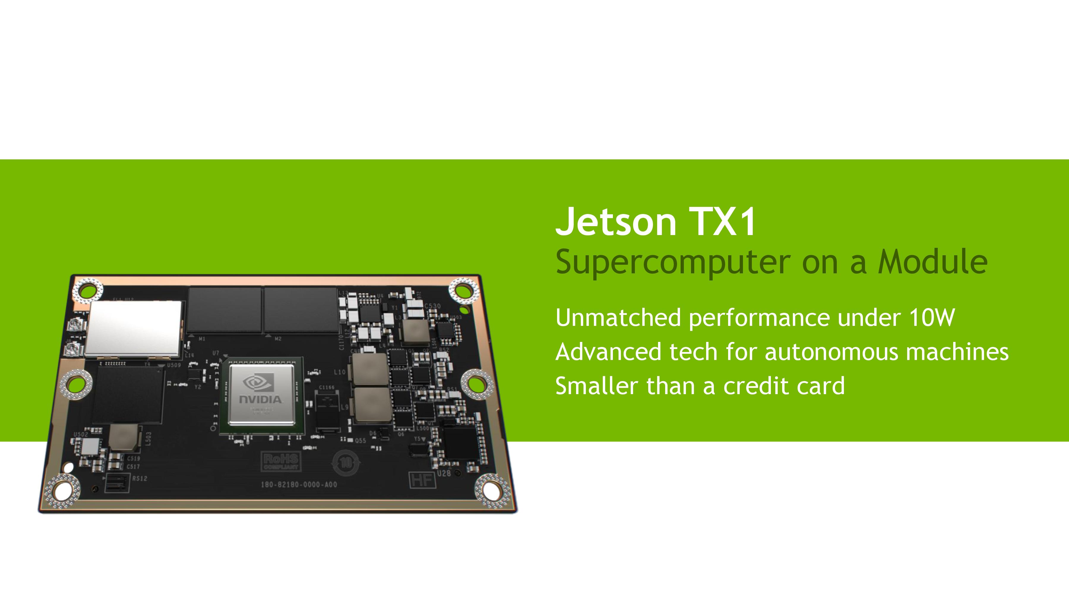
Moving on to the present, after announcing their latest-generation Tegra X1 SoC at CES 2015 and integrating it into some of their own products over the past several months (Drive PX, SHIELD Console, etc) NVIDIA is now rolling out an updated Jetson product based on the X1. The latest Jetson, which NVIDIA is appropriately calling the Jetson TX1, is designed to refresh the platform with the more powerful Tegra X1 SoC and its full ARMv8 AArch64 CPU + Maxwell GPU capabilities. At the same time however, based on their unexpected success as a COTS product, NVIDIA has redesigned Jetson to better serve the COTS market while also continuing to serve the Tegra developer kit market.
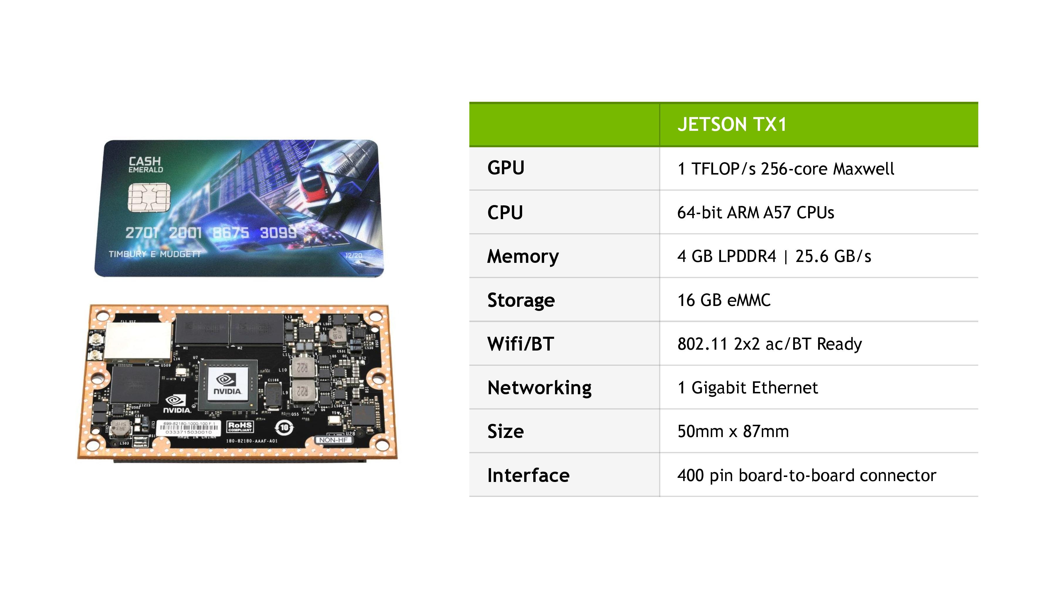
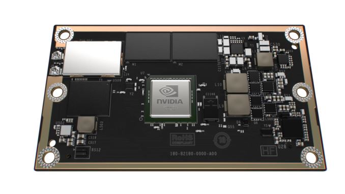
The end result is that for its TX1 iteration Jetson has been split in two, and now comes as stand-alone compute module with a separate carrier board for I/O. The Jetson TX1 module itself – which is for all practical definitions Jetson TX1 in its entirety – contains a full working TX1 system. NVIDIA tells us that Jetson TX1 should offer 2-3 times the performance of Tegra K1, particularly where the GPU is involved, and while we don’t have the CPU clockspeed some quick math on NVIDIA’s 1 TFLOPS claim puts the GPU clockspeed at 975MHz (assuming FP16) with the complete module rated for approximately 10W.
Otherwise along with the TX1 SoC, NVIDIA has attached 4GB of LPDDR4-3200, a 16GB eMMC flash module, a 2x2 802.11ac + Bluetooth wireless radio, and a Gigabit Ethernet controller. By providing a complete TX1 system on a board a bit smaller than a credit card, NVIDIA is looking to further the COTS usage of Jetson by giving product developers a smaller dedicated board specifically designed for COTS usage and quick integration into shipping products.
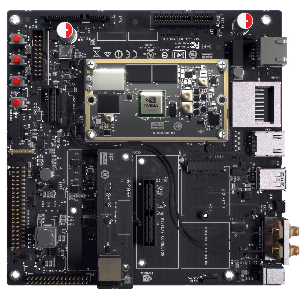
Meanwhile I/O connectivity is now provided by a separate board, be it a product-specific developer design or the official Jetson TX1 carrier board, with the Jetson TX1 using a 400 pin board-to-board connector to attach to other devices. Similar to the original Jetson TK1, the official Jetson TX1 carrier board is designed to offer TX1 as a development kit and contains a full suite of I/O including Ethernet, WiFi + BT antenna connectors, HDMI, USB, M.2, a large number of GPIOs, a camera serial interface with 5MP camera, and a PCIe 2.0 x4 slot. Relative to Jetson TK1, the newer TX1 includes more GPIOs, the camera, a full-size PCIe interface, and it can now work from a more traditional 3.3v power supply.
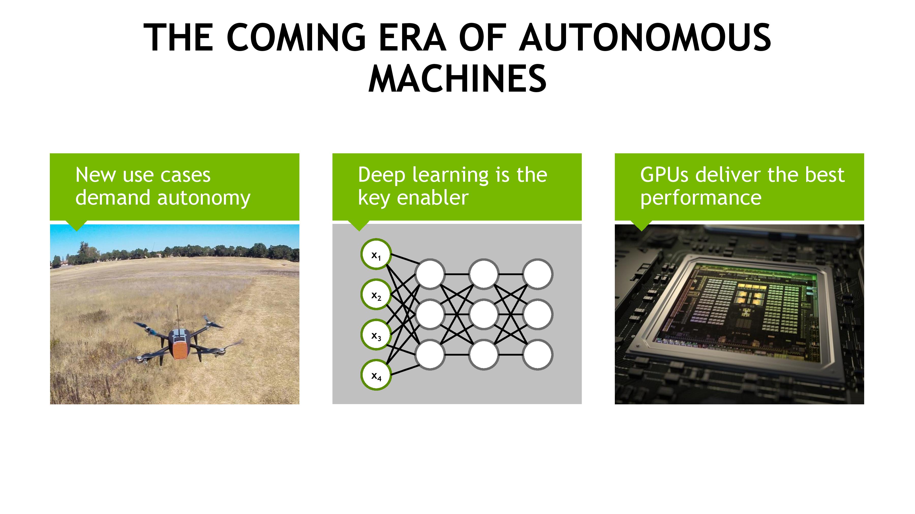
Moving on, not unlike TX1’s discrete GPU counterparts, with the Jetson TX1 platform NVIDIA is strongly focusing on machine learning and autonomous machines. The company believes that machine learning is the next great frontier for GPUs – both discrete and integrated – and is capitalizing on neural net research that has shown GPUs to be capable of both quickly training and quickly executing neural nets. This is an important differentiator for NVIDIA given their strengths in GPU development (both from a tech perspective and overall SoC GPU performance), and because it is a market that they feel no one else is truly aiming for (or at least competitive in) at this time. The Drive PX system already uses TX1 on this basis, and now with Jetson TX1 NVIDIA is looking to extend that relationship to a much wider group of developers.
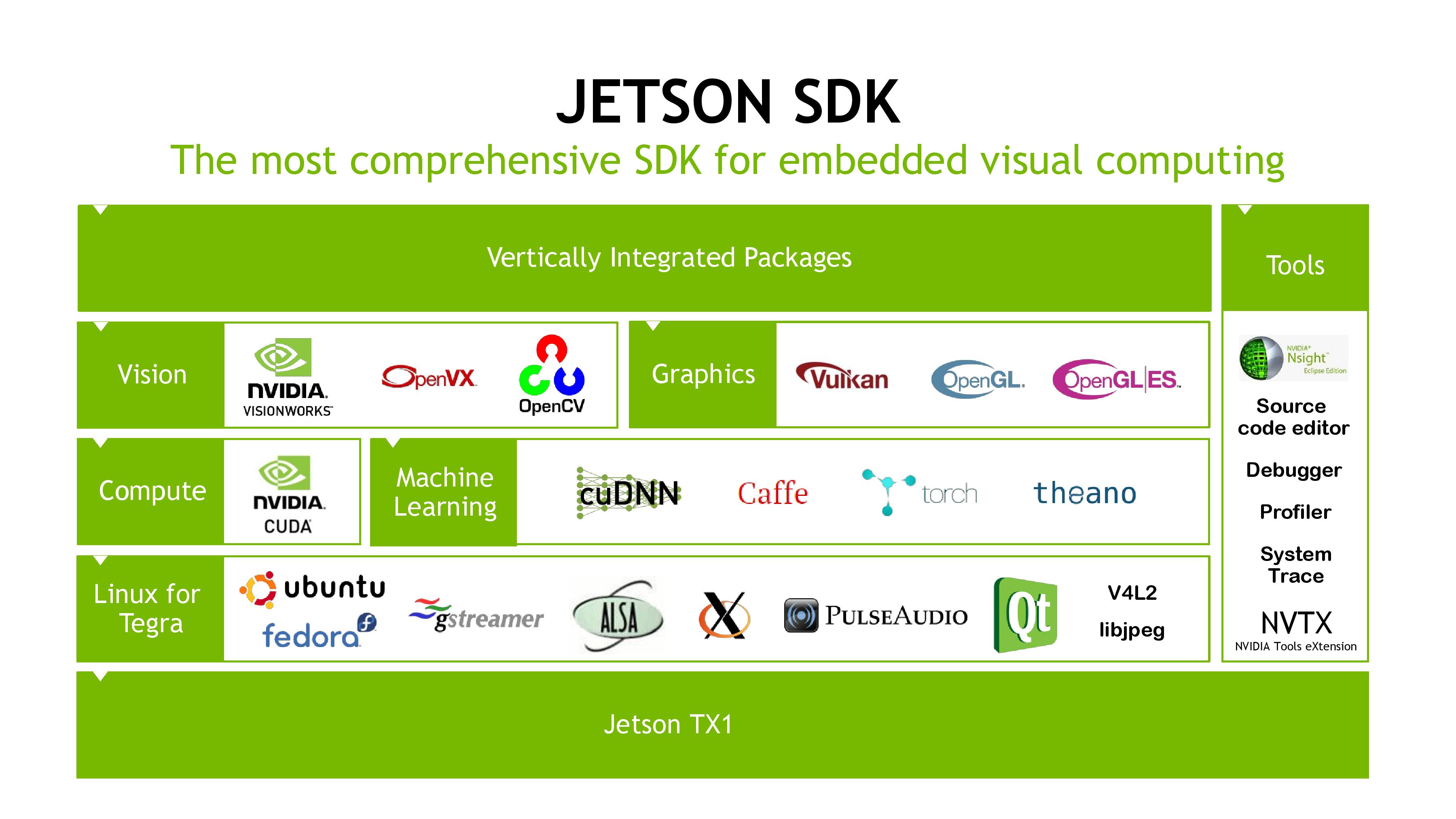
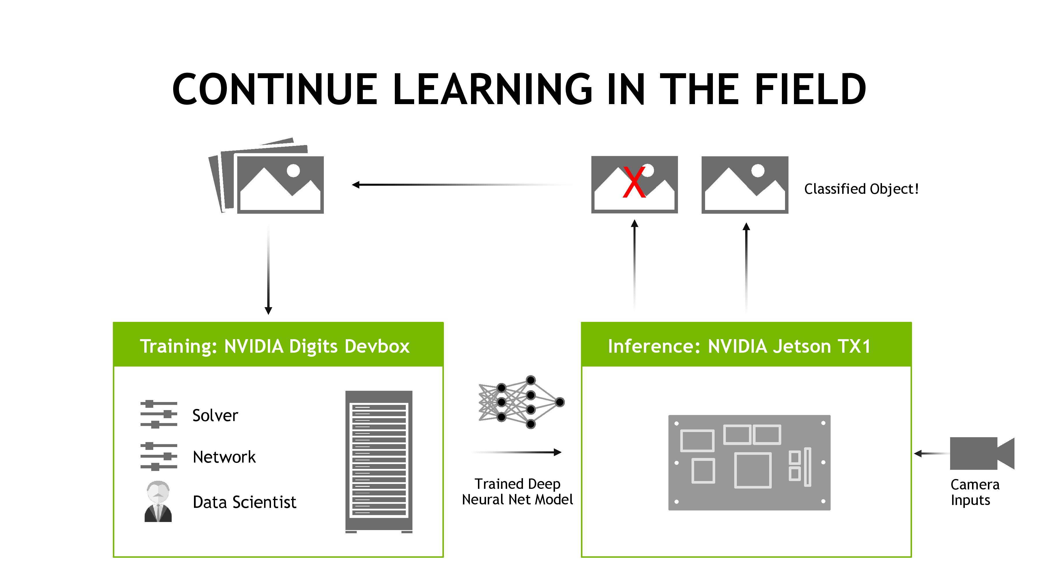
Similar to Jetson TK1 then, Jetson TX1 comes with a suite of software and SDKs in order to simplify the development process and to give developers a good starting point for implementing machine learning. Along with the Linux for Tegra environment, NVIDIA is including their cuDNN neural network library and VisionWorks computer vision toolkit. Coupled with other APIs and software packages such as OpenVX and various neural network systems, NVIDIA is aiming to make the Jetson SDK an ecosystem in and of itself.
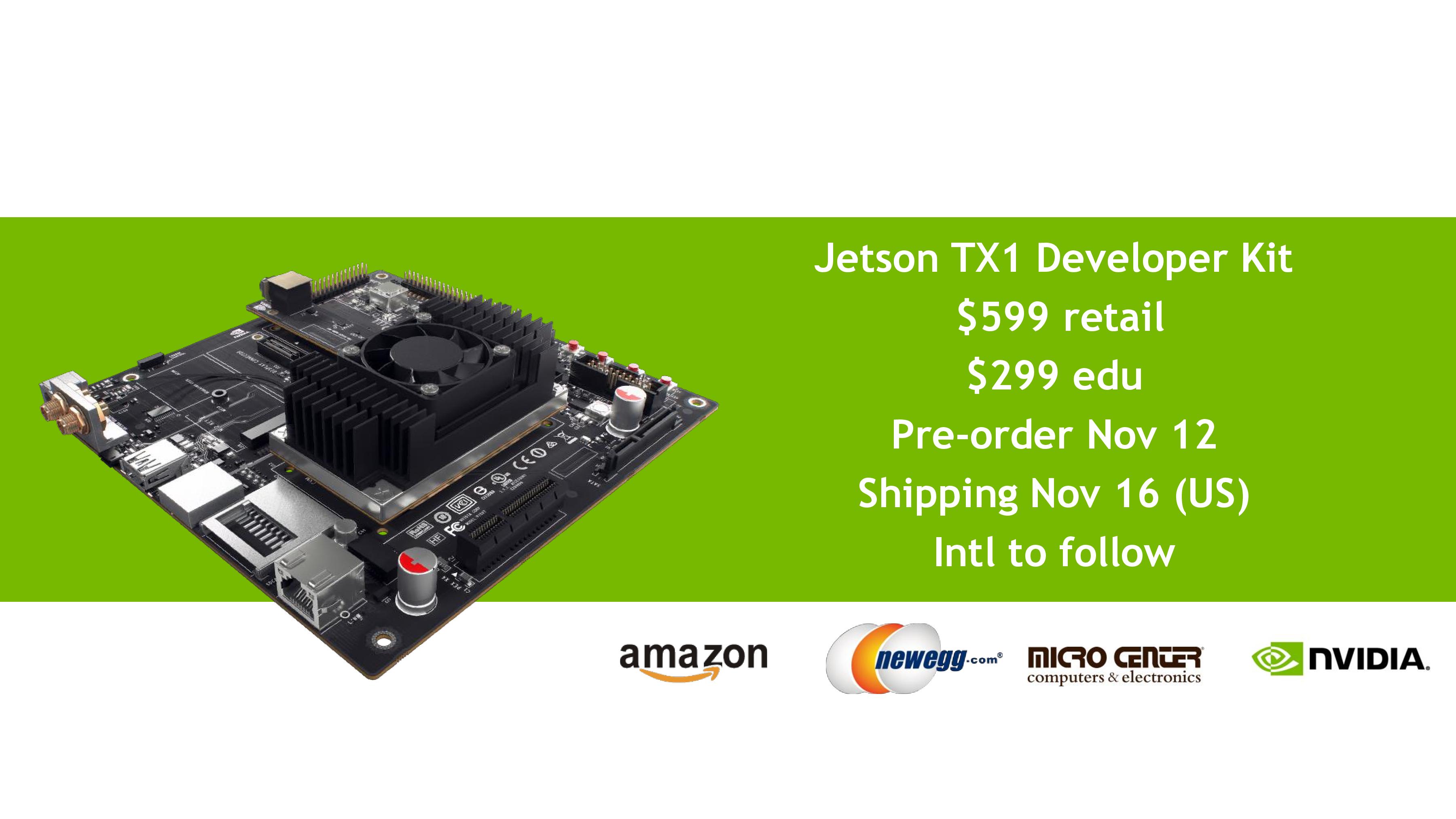
Finally, along with today’s announcement NVIDIA also unveiled the pricing and availability of the Jetson TX1 module and the full development kit. NVIDIA will begin taking pre-orders for the dev kit on the 12th with kits to start shipping as soon as the 16th, and will sell for $599 retail/$299 education. The dev kits will contain the module, carrier board, camera board, a heatsink-fan for cooling (which we’re told is grossly overpowered for TX1), and all of the necessary cables. Meanwhile the stand-alone Jetson TX1 module for use in commercial products will go on sale in Q1 of 2016, priced at $299 in 1K quantities.


34 Comments
View All Comments
ruthan - Tuesday, November 10, 2015 - link
How is difference between this board and rooted Nvidia Shield, is there some big advantage? Because HW is same except 400 pin connector and price is 2 times bigger..Braincruser - Tuesday, November 10, 2015 - link
These are development boards, their purpose is for you to develop a software around the hardware on the board for some specific purpose, usually in embedded development. I believe some of their previous boards were used in cars, for image recognition and system control.DanNeely - Tuesday, November 10, 2015 - link
If you're happy with the peripheral hardware built into a shield and don't need access to any hardware debugging features a rooted shield is going to be better. ie If you're going to install a linux distro someone else ported and either use off the shelf software or only write high level software a dev board isn't for you. If you need to write custom low level kernel code in general; or need to interface with some external hardware that's not related to watching cat tube or playing angry birds readily accessible IO headers, hardware debug points, and official support for flashing a new firmware when something goes wrong and your device fails to boot is worth many times the price difference between a dev kit and rooted consumer hardware.For people making medium sized hardware production runs splitting the dev kit into two parts, one with the core hardware, and a second with all the IO will offer significant hardware design savings. The most difficult/hard to make work right parts of building a system are on the small board with the CPU/ram/etc; designing a small IO board with the handful of ports you need is much less difficult work, and can be significantly cheaper to manufacture. Removing all the extra IO your application doesn't need also gives a free way to secure it against more casual tampering. (It won't keep out anyone who's determined to get in; but just denying USB/network/etc ports for them to plug cables into will stop a lot of people from trying.)
or just adding TX1 connector to an existing large board is
testbug00 - Tuesday, November 10, 2015 - link
Nvidia quoting 1TFLOP and not mentioning it's FP16. Terrific. Thanks Nvidia.There are standards which with specs are discussed, everyone uses FP32 for the most part for quoting GPUs.
Yojimbo - Tuesday, November 10, 2015 - link
It depends on the context. Here they are marketing it towards a segment with great interest in FP16 performance. It's not meant to play Fallout 4.testbug00 - Wednesday, November 11, 2015 - link
They didn't mention the FP16 on the slide. They obviously informed someone, or sites deduced it.Without it there you need to assume it's FP32.
HighTech4US - Wednesday, November 11, 2015 - link
assume: making an a** out of youMrSpadge - Wednesday, November 11, 2015 - link
Others would report FP16 performance if they were any faster at that than with FP32.ant6n - Tuesday, November 10, 2015 - link
All links in this article refer to other Anandtech articles.Yojimbo - Tuesday, November 10, 2015 - link
All whopping three of them.