The Intel Core i9-7980XE and Core i9-7960X CPU Review Part 1: Workstation
by Ian Cutress on September 25, 2017 3:01 AM ESTOpinion: Why Counting ‘Platform’ PCIe Lanes (and using it in Marketing) Is Absurd
It’s at this point that I’d like to take a detour and discuss something I’m not particularly happy with: counting PCIe lanes.
The number of PCIe lanes on a processor, for as long as I can remember, has always been about which lanes come directly from the PCIe root, offering full bandwidth and with the lowest possible latency. In modern systems this is the processor itself, or in earlier, less integrated systems, the Northbridge. By this metric, a standard Intel mainstream processor has 16 lanes, an AMD Ryzen has 16 or 20, an Intel HEDT processor has 28 or 44 depending on the model, and an AMD Ryzen Threadripper has 60.
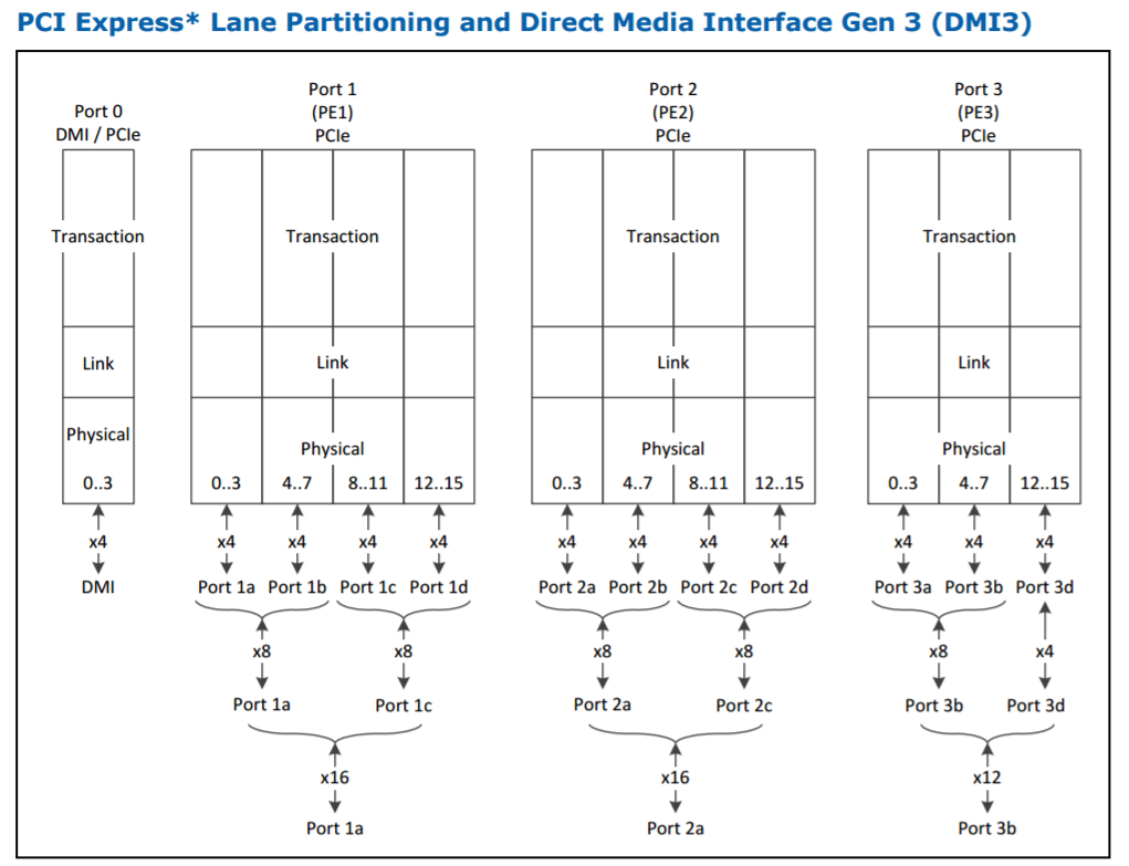
In Intel’s documentation, it explicitly lists what is available from the processor via the PCIe root complexes: here 44 lanes come from two lots of sixteen and one twelve lane complex. The DMI3 link to the chipset is in all but name a PCIe 3.0 x4 link, but is not included in this total.
The number of PCIe lanes on a chipset is a little different. Chipsets are for all practical purposes PCIe switches: using a limited bandwidth uplink, it is designed to carry traffic from low bandwidth controllers, such as SATA, Ethernet, and USB. AMD is limited in this regard, due to spending more time re-entering the pure CPU performance race over the last few years and outsource their designs to ASMedia. Intel has been increasing its PCIe 3.0 lane support on its chipsets for at least three generations, now supporting up to 24 PCIe 3.0 lanes. There are some caveats on what lanes can support which controllers, but in general we consider this 24.
Due to the shared uplink, PCIe lanes coming from the chipset (on both the AMD and Intel side) can be bottlenecked very easily, as well as being limited to PCIe 3.0 x4. The chipset introduces additional latency compared to having a controller directly attached to the processor, which is why we rarely see important hardware (GPUs, RAID controllers, FPGAs) connected to them.
The combination of the two lends itself to a variety of platform functionality and configurations. For example, for AMD's X399 platform that has 60 lanes from the processor, the following combinations are 'recommended':
| X399 Potential Configurations | |||
| Use | PCIe Lanes | Total | |
| Content Creator | 2 x Pro GPUs 2 x M.2 Cache Drives 10G Ethernet 1 x U.2 Storage 1 x M.2 OS/Apps 6 x SATA Local Backup |
x16/x16 from CPU x4 + x4 from CPU x4 from CPU x4 from CPU x4 from CPU From Chipset |
52 Lanes |
| Extreme PC | 2 x Gaming GPUs 1 x HDMI Capture Card 2 x M.2 for Games/Stream 10G Ethernet 1 x M.2 OS/Apps 6 x SATA Local Backup |
x16/x16 from CPU x8 from CPU x4 + x4 from CPU x4 from CPU x4 from CPU From Chipset |
56 Lanes |
| Streamer | 1 x Gaming GPU 1 x HDMI Capture Card 2 x M.2 Stream/Transcode 10G Ethernet 1 x U.2 Storage 1 x M.2 OS/Apps 6 x SATA Local Backup |
x16 from CPU x4 from CPU x4 + x4 from CPU x4 from CPU x4 from CPU x4 from CPU From Chipset |
40 Lanes |
| Render Farm | 4 x Vega FE Pro GPUs 2 x M.2 Cache Drives 1 x M.2 OS/Apps 6 x SATA Local Backup |
x16/x8/x8/x8 x4 + x4 from CPU x4 from CPU From Chipset |
52 Lanes |
What has started to happen is that these companies are combining both the CPU and chipset PCIe lane counts, in order to promote the biggest number. This is despite the fact that not all PCIe lanes are equal, they do not seem to care. As a result, Intel is cautiously promoting these new Skylake-X processors as having ’68 Platform PCIe lanes’, and has similar metrics in place for other upcoming hardware.
I want to nip this in the bud before it gets out of hand: this metric is misleading at best, and disingenuous at worst, especially given the history of how this metric has been provided in the past (and everyone will ignore the ‘Platform’ qualifier). Just because a number is bigger/smaller than a vendor expected does not give them the right to redefine it and mislead consumers.
To cite precedent: in the smartphone space, around 4-5 years ago, vendors were counting almost anything in the main processor as a core to provide a ‘full core count’. This meant that GPU segments became ‘cores’, special IP blocks for signal and image processing became ‘cores’, security IP blocks became ‘cores’. It was absurd to hear that a smartphone processor had fifteen cores, when the main general purpose cores were a quartet of ARM Cortex A7 designs. Users who follow the smartphone industry will notice that this nonsense stopped pretty quickly, partly due to anything being called a core, but some hints towards artificial cores potentially being placed in the system. If allowed to continue, this would have been a pointless metric.
The same thing is going to happen if the notion of ‘Platform PCIe Lanes’ is allowed to continue.


152 Comments
View All Comments
CrazyHawk - Tuesday, September 26, 2017 - link
"Intel also launched Xeon-W processors in the last couple of weeks."Just where can one purchase these mythical Xeon-W processors? There hasn't been a single peep about them since the "launch" week. I've only heard of two motherboards that will support them. They seem to be total vaporware. On Intel's own site, it says they were "Launched" in 3Q2017. Intel had better hurry up, 3Q will be up in 4 days!
samer1970 - Tuesday, September 26, 2017 - link
I dont understand why intel disables ECC on their i9 CPU , they are losing low budget workstation buyers who will 100% choose AMD threadripper over intel i9..Even if they are doing this to protect their xeons chips ,they can enable non buffered ECC and not allow Registered ECC on the i9 problem solved. unbuffered ECC has Size limitation and people who want more RAM will go for xeons.
Remember that their i3 has ECC support , but only the i3 ...
intel , you are stupid.
vladx - Wednesday, September 27, 2017 - link
Newsflash, these chips don't target "low budget workstation buyers". Golden rule is always: "If you can't afford it, you're not the target customer.".samer1970 - Wednesday, September 27, 2017 - link
Thats not a Golden Rule anymore with the Threadripper chips around . it is called "Stupid rule" ...They are allowing AMD to steal the low budget workstation buyers by not offering them an alternative to choose from.
vladx - Wednesday, September 27, 2017 - link
The "low budget workstation buyers" as you call them are a really insignificant percentage of an already really small piece of the huge pie of Intel customers.samer1970 - Wednesday, September 27, 2017 - link
who told you so ? Most engineering students at universities need one , and Art Students who render alot as well. all these people will buy threadripper CPU and avoid intel , for intel xeon are 50% more expensive .andI dont cae about the percentage in intel Pie ... hundreds of thousands student enter uiviersites around the world each year . Low percentage or not they are alot ...
how much do you think a low budget workstation costs ? they start from $3000 ... and with xeon Pricing , it will be very difficult to add alot of RAM and a good workstation card and fast SSD .
esi - Wednesday, September 27, 2017 - link
What's the explanation for some of the low scores of the 7980XE on the SPECwpc benchmarks? Particularly Poisson, where the 6950X is 3.5X higher.ZeDestructor - Wednesday, September 27, 2017 - link
Most likely cache-relatedesi - Wednesday, September 27, 2017 - link
Maybe. But one that really makes no sense is the Dolphin 5.0 render test. How can the 7980XE take nearly twice as long as the 7960X?esi - Wednesday, September 27, 2017 - link
So I ran the Poisson benchmark on by 6950X. It uses all 10 cores (20 h/w threads), but can be configured to run in different ways: you can set the number of s/w threads per process. It then creates enough processes to ensure there's one s/w thread per h/w thread. Changing the s/w threads per processes significantly effects the result:20 - 1.34
10 - 2.5
5 - 3.31
4 - 3.47
2 - 3.67
1 - 0.19
Each process only uses about 2.5MB of RAM. So the 1-thread per process probably has a low result as this will result in more RAM usage than L3 cache, whereas the others should all fit in.
Would be interesting to see what was used for the 7980/7960. Perhaps the unusual number of cores resulted in a less than optimal process/thread mapping.