Intel 12th Gen Core Alder Lake for Desktops: Top SKUs Only, Coming November 4th
by Dr. Ian Cutress on October 27, 2021 12:00 PM EST- Posted in
- CPUs
- Intel
- DDR4
- DDR5
- PCIe 5.0
- Alder Lake
- Intel 7
- 12th Gen Core
- Z690
Over the past few months, Intel has been drip-feeding information about its next-generation processor family. Alder Lake, commercially known as Intel’s 12th Generation Core architecture, is officially being announced today for a November 4th launch. Alder Lake contains Intel’s latest generation high-performance cores combined with new high-efficiency cores for a new hybrid design, along with updates to Windows 11 to improve performance with the new heterogeneous layout. Only the six high-performance K and KF processor variants are coming this side of the New Year, with the rest due for Q1. We have specifications, details, and insights ahead of the product reviews on November 4th.
Today’s announcement also coincides with Intel’s InnovatiON virtual event happening today and tomorrow. This event is, as described in a number of press releases, a mini-Intel Developer Forum (IDF) event designed to emulate a small part of the highly prized annual conference that the company culled in 2017. As part of the event, there are 60+ sessions designed to cover new technology such as AI, networking, custom silicon, programming technologies/challenges, and introduce developers to more of Intel’s ecosystem. It includes a day one keynote from CEO Pat Gelsinger and other executives to share the new hardware announcements, and a day two keynote from CTO Greg Lavender on the software side. The goal was for this event to be in-person, which is usually where the most value came from the old IDF event, however this is the first attempt to revive the format.
Six Alder Lake CPUs, $589 For Core i9
The first things we’ll go into are the new CPUs that Intel is announcing today: the overclockable models of Intel 12th Gen Core. As with previous launches, we have Core i9, Core i7, and Core i5, with the key highlights including new support for DDR5, PCIe Gen 5, new overclocking features, and a change in how Intel is promoting its Thermal Design Power (TDP).
This is the table:
| Intel 12th Gen Core, Alder Lake | |||||||||
| AnandTech | Cores P+E/T |
E-Core Base |
E-Core Turbo |
P-Core Base |
P-Core Turbo |
IGP | Base W |
Turbo W |
Price $1ku |
| i9-12900K | 8+8/24 | 2400 | 3900 | 3200 | 5200 | 770 | 125 | 241 | $589 |
| i9-12900KF | 8+8/24 | 2400 | 3900 | 3200 | 5200 | - | 125 | 241 | $564 |
| i7-12700K | 8+4/20 | 2700 | 3800 | 3600 | 5000 | 770 | 125 | 190 | $409 |
| i7-12700KF | 8+4/20 | 2700 | 3800 | 3600 | 5000 | - | 125 | 190 | $384 |
| i5-12600K | 6+4/16 | 2800 | 3600 | 3700 | 4900 | 770 | 125 | 150 | $289 |
| i5-12600KF | 6+4/16 | 2800 | 3600 | 3700 | 4900 | - | 125 | 150 | $264 |
Each processor has a number of performance cores (P-cores) and efficiency cores (E-cores). The P-cores have SMT, whereas the E-cores do not, so we’re dealing with non-standard numbers of total threads. Inside the system, the P-core threads, E-core threads, and SMT threads are categorized for performance and efficiency, which we’ll get to later in the article. But with a new hybrid design also comes with new ways to showcase frequencies, and each set of cores will have its own base frequency and turbo frequency. The way power is marketed and used has also changed, designed to be clearer.
All processors will come with 16 lanes of PCIe 5.0 from the processor, and an additional 4 lanes of PCIe 4.0 for storage. Memory support is listed as both DDR5-4800 and DDR4-3200, although systems will only support one or the other, for a maximum of 128 GB. The K processors also feature 32 EUs of Intel’s Xe-LP graphics, designated as UHD Graphics 770. Prices will start at $264 for the base Core i5 model, up to $589 for the top Core i9 model.
Core i9-12900K/KF
For the Core i9-12900K, if we work from the ground up, the E-cores have a base frequency of 2.4 GHz but will turbo up to 3.9 GHz; the P-cores have a base frequency of 3.2 GHz, and an all-core turbo of 5.1 GHz. The P-cores that are considered the best (aka favored cores) will turbo up to 5.2 GHz.
With all the cores active, the system has all 30 MiB of L3 cache available. Intel lists the base power as 125 W, with a turbo power of 241 W. The 1000-unit price for the K model is $589, and the KF model without integrated graphics as $564. As these are 1000-unit prices, retail is expected to be $10-$50 higher, depending on how Intel bundles the chip.
| Compare at $550-$600 | |||||||
| AnandTech | Cores P+E/T |
P-Core Base |
P-Core Turbo |
IGP | Base W |
Turbo W |
Price $1ku |
| i9-12900K | 8+8/24 | 3200 | 5200 | 770 | 125 | 241 | $589 |
| R9 5900X | 12/24 | 3700 | 4800 | - | 105 | 142 | $549 |
On price, the Core i9 parts are up against the Ryzen 9 5900X (12C/24T, 3.7-4.8 GHz) at $549. Intel has more actual cores, but AMD has more high-performance cores. At 105W/142W, AMD has the power advantage, but Intel has PCIe 5.0 and DDR5 support, with the K also having integrated graphics.
Core i7-12700K/KF
For the Core i7, Intel has removed one set of four E-cores, and also reduced the L3 cache to 25 MiB. This leads to an 8P+4E design, with 20 total threads. Over the Core i9, the E-cores in the Core i7 have a higher base frequency at 2.7 GHz, but a lower turbo frequency of 3.8 GHz. The P-cores are also higher at 3.6 GHz, but the turbo is 4.9 GHz, with the favored core at 5.0 GHz.
Intel lists the base power here as the same 125 W, but the turbo power is only 190 W. Pricing is at $409 for the K model in 1000-unit quantities, with the KF at $384. This puts it favorably against the Ryzen 7 5800X.
| Compare at $400-$450 | |||||||
| AnandTech | Cores P+E/T |
P-Core Base |
P-Core Turbo |
IGP | Base W |
Turbo W |
Price $1ku |
| i7-12700K | 8+4/20 | 3600 | 5000 | 770 | 125 | 190 | $409 |
| R7 5800X | 8/16 | 3800 | 4700 | - | 105 | 142 | $449 |
On price, the Core i7 $40 is cheaper. While both have eight performance cores, the addition of four efficiency cores on the i7 is an interesting twist that might come down to how threads are managed and how Intel’s single-core performance changes when threads are loaded. At 125 W, AMD still has the on-paper power advantage, but real-world testing will see if Intel is drawing level.
Core i5-12600K/KF
The Core i5-12600K loses two P-cores compared to the Core i7, for a 6P+4E design totaling 16 threads. What we have here is a design that effectively replaces 2P cores for a 4-core E complex, and so up against the traditional 8C/16T chips will be an interesting scenario – even against Intel’s previous flagship, the 8C/16T Core i9-11900K.
The frequencies here change a bit as before, with an increased E-core base but lower E-core turbo. The P-core base is up too, but the P-core turbo is the same 4.9 GHz – the difference to the i7 is that there is no preferred core turbo mode.
| Compare at ~$300 | |||||||
| AnandTech | Cores P+E/T |
P-Core Base |
P-Core Turbo |
IGP | Base W |
Turbo W |
Price $1ku |
| i5-12600K | 6+4/16 | 3700 | 4900 | 770 | 125 | 150 | $289 |
| R5 5600X | 6/12 | 3700 | 4600 | - | 65 | 88 | $299 |
The price competition for the Core i5-12600K is going to be one of AMD’s best sellers. The Ryzen 5 5600X is effectively the same price, and uses a 6C/12T design, rather than Intel’s 6P4E/16T. If that looks confusing, we’ve got a fun few years ahead. It should be noted though that AMD’s hardware has a TDP of 65W, almost half of the base 125 W power listed for the Core i5. The comparison of performance against efficiency is going to be an important one.
Chipset and Motherboards
Inside each processor, alongside the 16x PCIe 5.0 lanes for add-in cards and 4x PCIe 4.0 lanes for storage, is an additional link to the chipset. Intel lists this as a DMI 4.0 x8 link, as they use a custom protocol over an effective PCIe physical connection – we asked Intel, and they said the link is rated for 15.76 GB/s, which means the chipset can take two PCIe 4.0 x4 drives at peak before getting near to that limit. This is doubled compared to Z590, which was only 7.88 GB/s.
Today Intel is only announcing its Z690 chipset, built on Intel’s 14nm, and the motherboard manufacturers have about 60+ models to launch in the upcoming week. The processors use a new LGA1700 socket, which means everyone buying the new CPUs also need a new motherboard. Most of the big motherboard companies are holding their own product announcement events, so keep a lookout for those. Each motherboard will support either DDR5 or DDR4, not both, along with enhanced overclocking - more detail on that below.
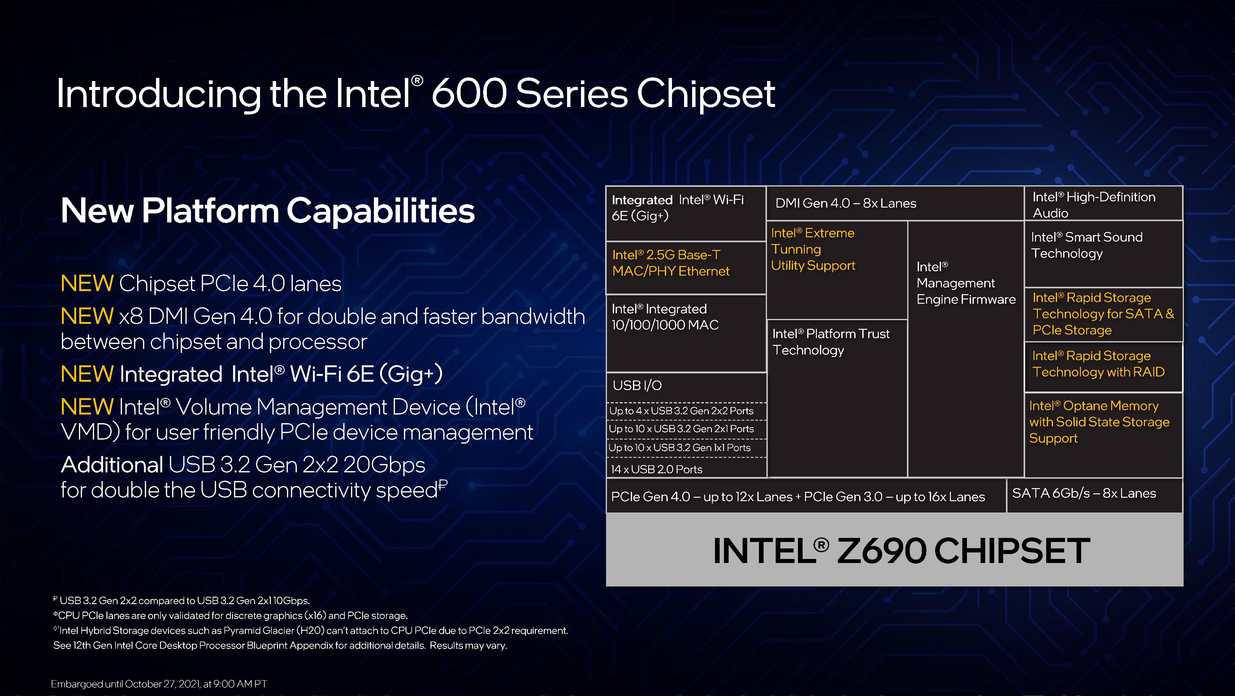
The Z690 chipset will have 12x PCIe 4.0 lanes and 16x PCIe 3.0 lanes, some of which will be earmarked for general IO use. This includes up to four 20 Gb/s USB ports, up to ten 10 Gb/s USB ports, up to ten 5 Gb/s USB ports, and up to fourteen USB 2.0 ports (although not all at the same time). There are eight SATA ports, along with support for Intel’s onboard RAID. The PCIe storage also now uses Intel’s Volume Management Device (VMD) to assist with PCIe management.
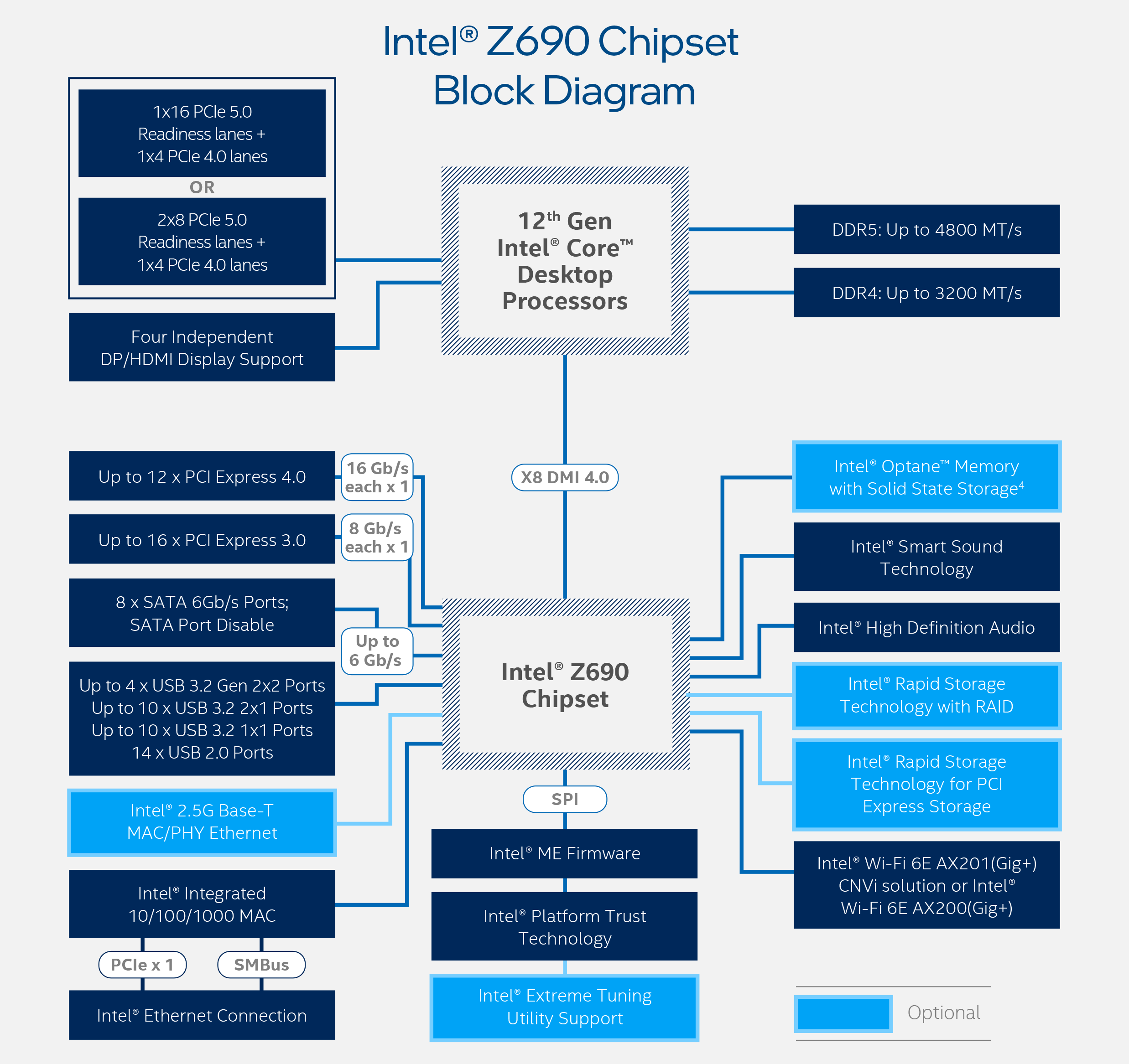
Intel lists an integrated Wi-Fi 6E MAC in the chipset as well, requiring the respective PHY and RF connected over CNVi, which is a proprietary Intel interface – any motherboard manufacturers wanting to use other Wi-Fi 6 solutions will have to directly connect via PCIe as they can’t use the closed standard.
Intel also lists 2.5G Base-T support for wired Ethernet, although that’s a bit of a misnomer here – it’s simply an attached PCIe device using the above-mentioned lanes, and the MAC/PHY still needs to be purchased. This is a similar tactic to previous announcements – users could also add a RAID card in a similar fashion or an FPGA accelerator, however Intel doesn’t highlight those.
Intel’s chipsets employ a great deal of port flexibility – it is essentially a big PCIe switch with a few added extras. It means almost everything that can be attached to a PCIe bus can be used. But with previous generations, there are going to be some limitations with the high-speed IO lanes (such only certain lanes can be used for SATA or Ethernet, limiting perhaps the number of PCIe x4 slots), but some combinations will be better supported than others. Users looking for Thunderbolt 4 support will have to find motherboards with an added controller, as the Alder Lake desktop processors do not have it built-in like the mobile versions.
Intel has not specified the TDP of the Z690 chipset, however we’re yet to see a motherboard with active cooling, so it’s likely to be in that 7-12W range as with previous generations. We expect to see Z690 motherboards range in price from $200 up to $700+, similar to Z590 pricing.
No More TDP: Base Power and Turbo Power
In the past, Intel promoted its processor power as a single number: TDP (Thermal Design Power*). The issue wasn’t so much that this number was wrong, it was because it lacked massive context that wasn’t communicated to anyone. Arguably it took us several years to find out what it really meant, especially in relation to its turbo.
*Technically TDP is defined differently to power consumption, however they are effectively interchangeable at this point, both in common parlance and Intel documentation.
What Intel was promoting wasn’t the power consumption in regular operation, but the guaranteed power consumption for the base processor specifications. That means if a user purchased a six-core processor, base frequency at 3.0 GHz, and a TDP of 65 W, then those are the only specifications that were covered under warranty. Even if the box showcased that the processor was capable of enabling a turbo up to 4.0 GHz, that wasn’t guaranteed. Beyond that, the power consumption of the turbo mode wasn’t specified either, so if the same processor went up to 30-50% higher than 65 W, there was no explicit number from Intel, aside from digging through specification sheets that sometimes weren’t even public, to get a number to help build cooling into the system. It also meant that reviews of hardware that were labeled as 125 W, but consumed 250W+ in turbo mode, weren’t able to accurately demonstrate the scope of the product without additional power monitoring. It got to a point where Intel’s power consumption under turbo became a bit of a meme, and enthusiasts got annoyed that Intel buried this information away.
That changes with Alder Lake. Intel is now acknowledging that its turbo mode does indeed have a power increase, and is providing that number alongside the regular set of numbers. To that end, the base ‘TDP’ number of previous generations is gone, and we get two numbers to talk about:
- Processor Base Power (Base): Guaranteed Peak Power at Base Frequency
- Maximum Turbo Power (Turbo): The Maximum Power at full turbo mode that is in spec
So for example, the Processor Base Power (Base) for the Core i9-12900K is set at 125 W. The Maximum Turbo Power is 241 W. This means that systems using this processor will be able to boost up to 241 W if the system is set up to do so, and that is within specification.
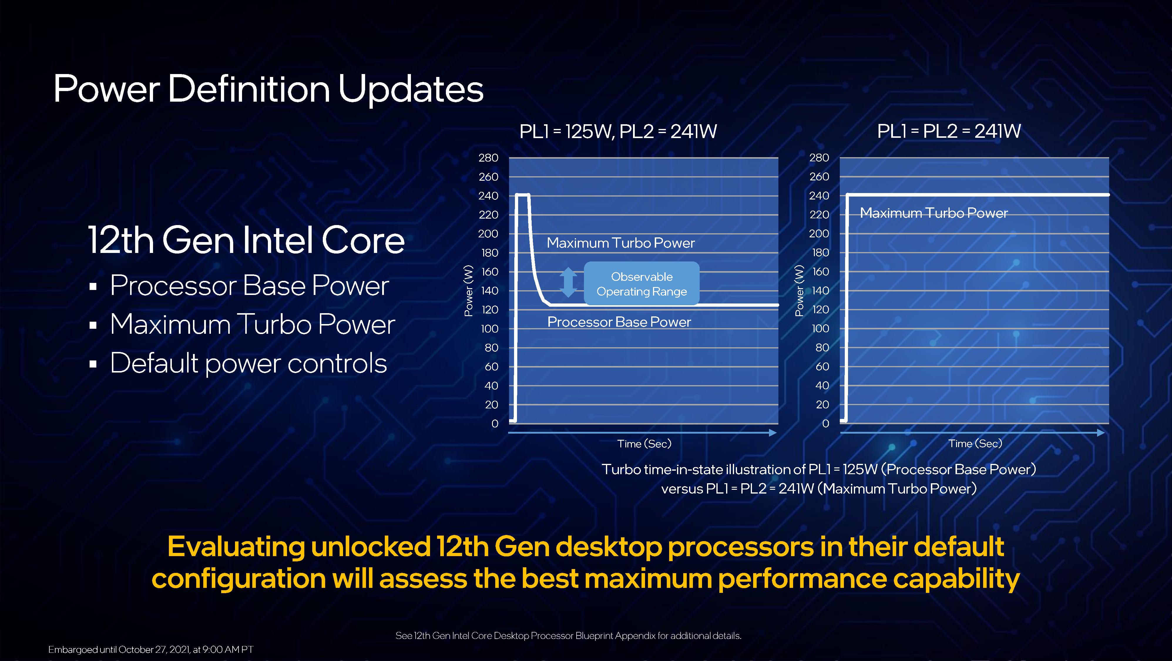
For the six processors being announced today, there’s also an added bonus. Under the previous regime, how long a processor could spend in that higher power mode was limited. Intel had a specification for this, which to be honest most motherboard manufacturers ignored anyway, because that length of time was only a guideline, not a rigid specification, and it didn’t break the warranty. Intel is now so confident in its turbo performance, that the new K processors have a default guideline of an unlimited turbo. It should be noted that when Intel launches the rest of the Alder Lake processors, this won’t always be the case.
For users who understand the former PL1/PL2 methodology, it still technically exists under the hood here, where Base is PL1 and Turbo is PL2, but Tau is effectively infinite for K processors.
More in this overview:
- Cache and Hybrid Designs
- Thread Director
- DDR5: Support, XMP, New Features
- Packaging and Overclocking
- Performance and Conclusions


395 Comments
View All Comments
Spunjji - Friday, October 29, 2021 - link
62MTr/mm^2 (Renoir) vs 53MTr/mm^2 (Ice Lake).Efficiency comparisons between those two chips aren't flattering, either - same goes for Tiger Lake and Cezanne. If you limit both to 15W, AMD win more often than not. Intel need 28W+ (4C) and 60W+ (8C) to open up a performance lead.
Wrs - Saturday, October 30, 2021 - link
Comparing apples and oranges. Renoir was 8 Zen2 cores with HT disabled. Ice Lake-U was 4 Sunny Cove with HT enabled. Of course Renoir was better at MT, but slower at ST. It's a basic design tradeoff. An exaggerated example would be Intel shipping 12 Atom cores instead of 4 Willow Cove. Similar die area, but higher efficiency! Also more complaints about slowdowns.Also note Zen3's are on the same process as Zen 2, whereas ADL is on a newer process than I
Wrs - Thursday, October 28, 2021 - link
And the power density difference is obvious and deliberate. Zen3 power is concentrated on the CCDs, ADL on the other hand is one piece of silicon over twice the size. Then measure the elevation difference between PCB and IHS on a Ryzen 5000, compare to reviewers doing the same on ADL. Thinner interface = better heat dissipation. That assumes other factors equal. Intel specifically talks about thin solder and thicker IHS, which is a further bonus because copper IHS has 5x the thermal conductivity of indium solder.Oxford Guy - Thursday, October 28, 2021 - link
Indium is also expensive and a depleting resource. Copper is rather more abundant.mode_13h - Friday, October 29, 2021 - link
Is it plausible that the thick IHS is there mostly as extra thermal mass to facilitate the PL2 turbo boost?I wonder if we'll ever see a CPU use a vapor chamber instead of solder + IHS. Just etch capillaries directly into the die surface and use some non-conductive liquid. Even solid copper is no match for the thermal conductivity of a vapor chamber!
Wrs - Tuesday, November 2, 2021 - link
@mode_13h The thicker IHS is to reduce the bending moment, to compensate for the thinner solder leaving the die more fragile. Solder is a soft metal, but the chip is ceramic, cracks like a ceramic tile. And if they needed more thermal mass they'd fill in the void between IHS and substrate, where the chip isn't.On the vapor chamber idea... install heatsink wrong, chip explodes?
mode_13h - Friday, November 5, 2021 - link
> if they needed more thermal mass they'd fill in the void between IHS and substrate,> where the chip isn't.
Compared to the added volume of the IHS, I don't see that extra space as being very significant.
> On the vapor chamber idea... install heatsink wrong, chip explodes?
Huh? Vapor chambers are like heat pipes. Yes, it'd have to be mechanically strong, but I don't see why this approach would be significantly weaker than the CPUs we have today. And so what you're saying is that if you push down too hard on this, it'd fail just like if you push down too hard on a conventional CPUs. The risk is in breaking the substrate.
Now, if you don't know about heatpipes, they're significantly *below* atmospheric pressure, at room temperature. So, while a CPU is cold, the real risk would be cracking it and creating a leak. The fluid would have to be something not terribly hazardous, in case it did leak out. However, I think phase-change cooling systems already commonly employ relatively benign fluids for similar purposes.
Spunjji - Friday, October 29, 2021 - link
I'm aware of how these things work. As I said on your other comments, Intel are doing these things (die thinning, solder thinning) because they have to, thanks to the amount of power they need to dissipate to stay competitive. Up until Comet Lake they were slapping thermal paste under the IHS and calling it a day. I approve of these changes and I have little doubt that AMD will start implementing similar techniques as and when they need to (TDPs in general are on an upward trend).GC2:CS - Wednesday, October 27, 2021 - link
Well exciting times coming up will all the new CPU competition ramping up.I am jsut curious how can the “little core” drop off only about 20% perf while being 1/4 the size ?
That is not a little core at all. More like lower clocked P core. If I remember corectly Apple little cores are only 1/3 of P cores and quite insignificant in MT workloads.
nandnandnand - Wednesday, October 27, 2021 - link
Who knows. I think we still need official word or die shots to confirm the relative die size of the efficiency cores. They have 40% of the L2 cache and no hyper-threading which should make a difference."A segment contains either a P-core or a set of four E-cores, due to their relative size and functionality. Each P-core has 1.25 MiB of private L2 cache, which a group of four E-cores has 2 MiB of shared L2 cache."