Intel Expands 12th Gen Core to Ultraportable Laptops, from 5-cores at 9 W to 14-cores at 28 W
by Dr. Ian Cutress on January 19, 2022 8:00 AM EST
Over the years Intel has prided itself on its ability to provide processors that fit into the ultraportable, professional market. We’re talking thin and light designs with obscene levels of performance and battery life for the form factor. It’s so important to Intel, that over the years they’ve produced several design and validation standards relating to how the best ultraportables should be developed, such as low power displays, the best connectivity standards, and approaching all-day battery life. It surprised me somewhat that Intel didn’t really discuss its next generation of processors for these devices at CES at the beginning of the year, focusing their keynote almost entirely on the 45 W prosumer and workhorse designs instead. To find out about the more mainstream and ultraportable silicon, we had to dig into the back end of our press deck to get details.
Core Counts Get Crazy
Intel typically addresses the ultraportable market with its U-series processors, which all end in a U in the product name. Depending on the exact configuration, these processors started with dual-core parts at 9 W, scaling to quad-core at 28 W. This time around, Intel is changing it up, partly due to the new Hybrid core design.
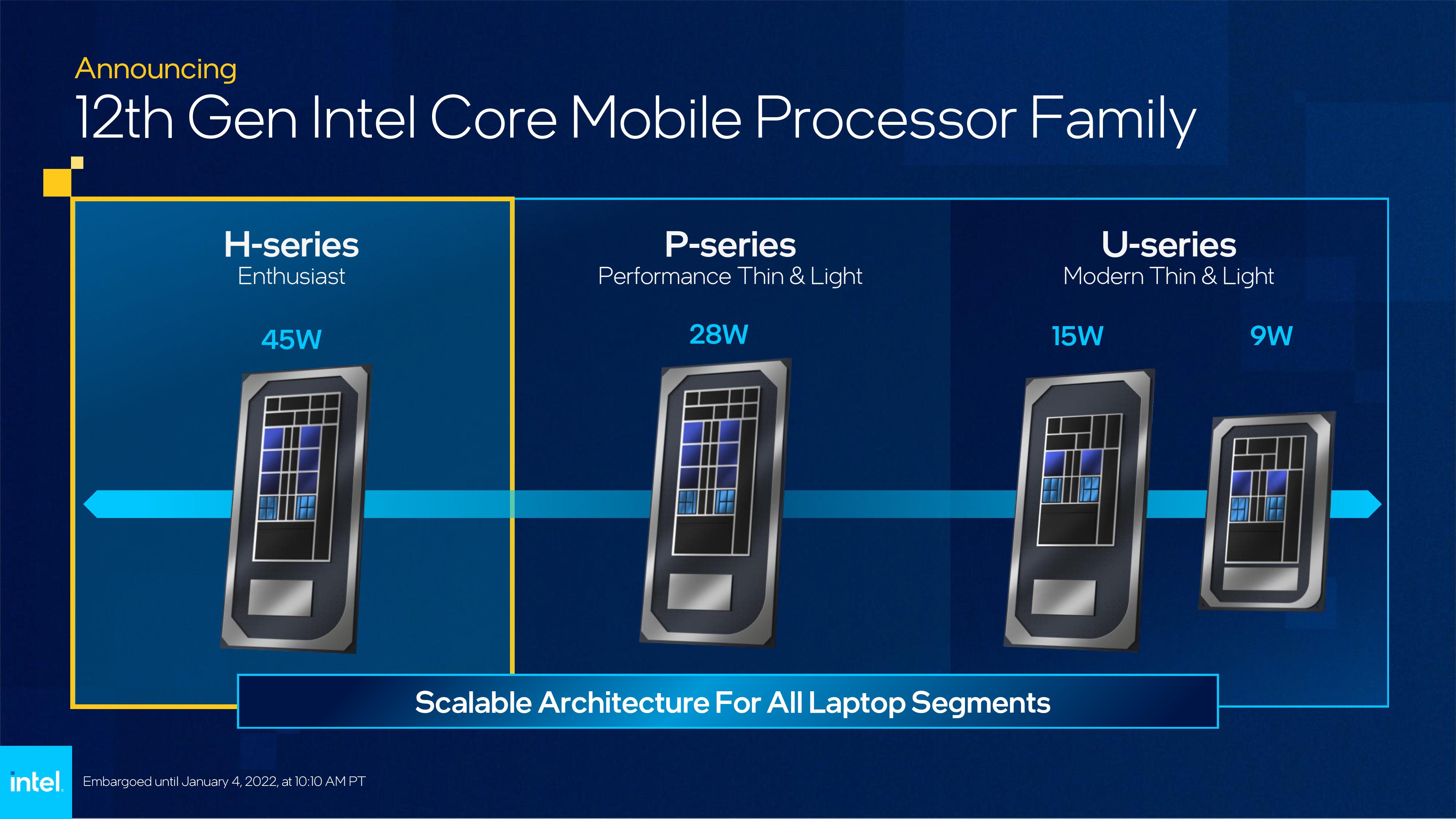
Starting with the low power processor at 9 W, Intel classifies this as a U-series processor featuring two performance cores, eight efficiency cores, and 96 execution units of graphics in the silicon. As with the ultra low power Tiger Lake processors, this uses an Intel design known as ‘BGA Type4’, or ‘UP4’, that combines both the CPU and the chipset on the same package. and is the smallest such processor package that they offer.
At 15 W, we’re in the more traditional U-series that we are familiar with. The package size increases to what Intel calls BGA Type3, or UP3, but you’ll notice that the CPU layout looks identical to the 9 W version. That’s because it is the same – up to two performance cores and eight efficiency cores, then 96 execution units on graphics. This is going to be important: for a market readily served today by the Core i9-1195G7 – an 11th Gen 15 W processor with four large cores – Intel is pivoting to fewer performance cores and more efficiency cores for their 12th Gen chips. It’s also worth noting that the chipset is also on die, but offers more functionality than the 9 W chips.
Then as we move to the higher powered parts, Intel is introducing a new series called P, designed to run at 28 W. Intel has technically used P before, but on the desktop, and then replaced it with F. In this case however, the P series stays in that UP3 form factor but gets the larger, more powerful silicon, with up to six performance cores, eight efficiency cores, and the same 96 EU graphics. The idea here is that a vendor can make a UP3 notebook and either equip it with a higher performance P-series chip or a lower power U-series at 15 W.
Perhaps this is why Intel kept this side of the Core 12th Gen away from the main presentation – we’re seeing a fundamental realignment of how the company is classifying its traditional 9/15/28 W segments. What used to be 4 core is now 2+8 core, and that expands into the processor lists as well, where we start with 5-core parts, and end at 14-core processors.
It’s also worth noting that the naming of these processors has changed from the previous generation – they are no longer getting G7, G4, or G1 suffixes to signify graphics configurations. Now Intel is only signifying power, using either a P or a U to respectively.
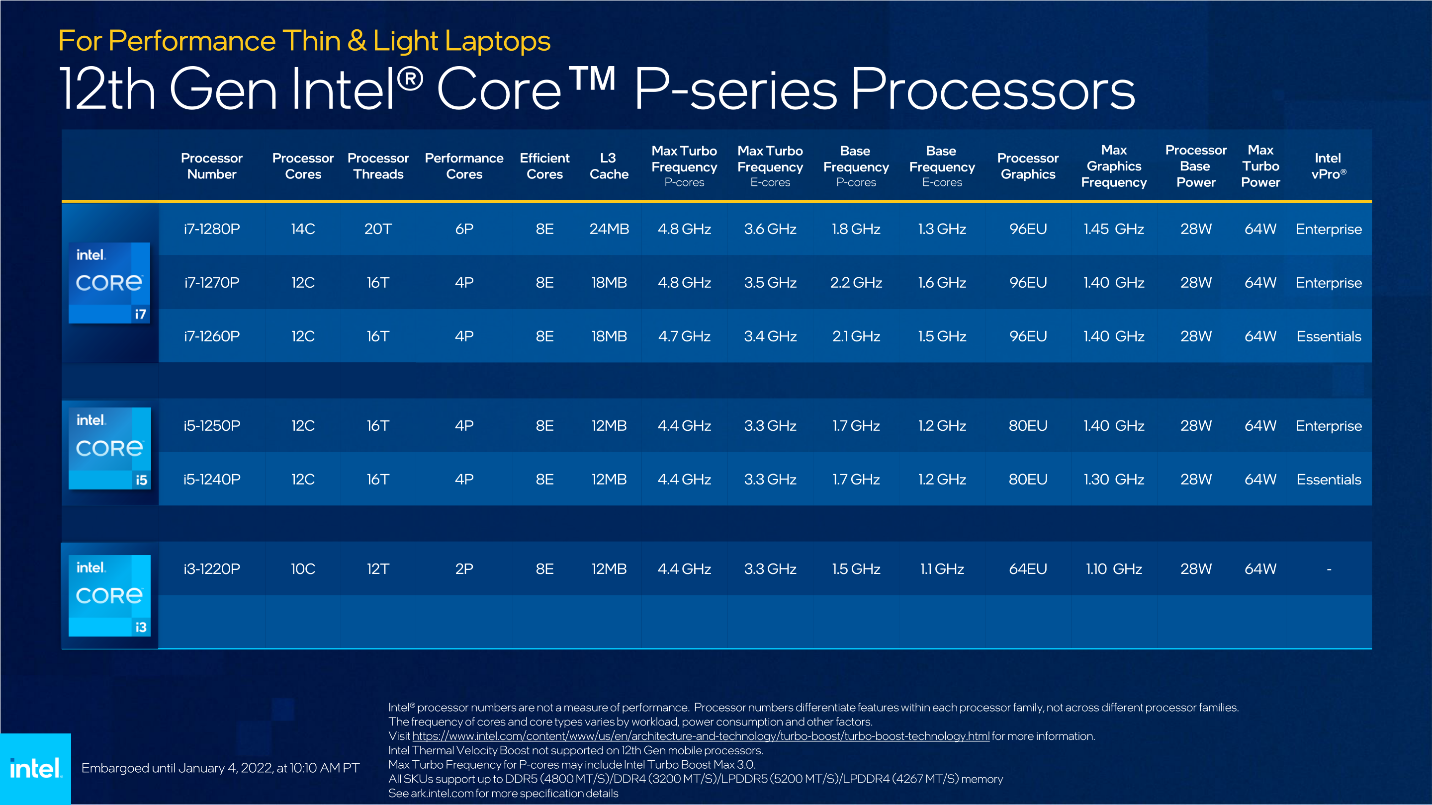
| Intel 12th Gen Core-P at 28 W (UP3) | ||||||||
| AnandTech | Core P+E |
Base E |
Turbo E |
Base P |
Turbo P |
GFX EUs |
GPU MHz |
L3 MB |
| i7-1280P | 6+8 | 1300 | 3600 | 1800 | 4800 | 96 | 1450 | 24 |
| i7-1270P | 4+8 | 1600 | 3500 | 2200 | 4800 | 96 | 1400 | 18 |
| i7-1260P | 4+8 | 1500 | 3400 | 2100 | 4700 | 96 | 1400 | 18 |
| i5-1250P | 4+8 | 1200 | 3300 | 1700 | 4400 | 80 | 1400 | 12 |
| i5-1240P | 4+8 | 1200 | 3300 | 1700 | 4400 | 80 | 1300 | 12 |
| i3-1220P | 2+8 | 1100 | 3300 | 1500 | 4400 | 64 | 1100 | 12 |
At the top of the P-series is the Core i7-1280P, and it’s the only P-series processor with everything enabled. It has six performance cores, eight efficiency cores, and offers a peak turbo frequency of 4.8 GHz. It has all the graphics cores running at a 1.45 GHz peak, and a max turbo power consumption of 64 W.
The other Core i7 parts, the i7-1270P and 1260P, lose two of the performance cores, and in exchange get extra base frequency on both performance and efficiency cores. The loss of two cores also reduces the L3 cache size from 24 MB to 18 MB, which is going to have an effect on some performance metrics, especially if these processors are paired with discrete graphics. Looking at this table, Intel should have made that i7-1280P at the top a Core i9 to differentiate it.
In the mid-range, the Core i5 processors have the same 4+8 core configurations as most of the i7 parts, but are reduced slightly on peak turbo frequency and graphics, coming down from 96 execution units to 80 execution units. This is a 16% drop, but the frequencies are still equivalent. Intel still lists these processors as 28 W Base, 64 W turbo.
Bringing up the rear is the Core i3-1220P, which offers only two efficiency cores and eight performance cores. Thie integrated graphics are also further cut back, with another drop to 64 execution units, but still the same 28-64 W power window. This Core i3-P looks very much like what the top Core i7-U processors will be in that configuration, but the Core i7-U are much more efficient.
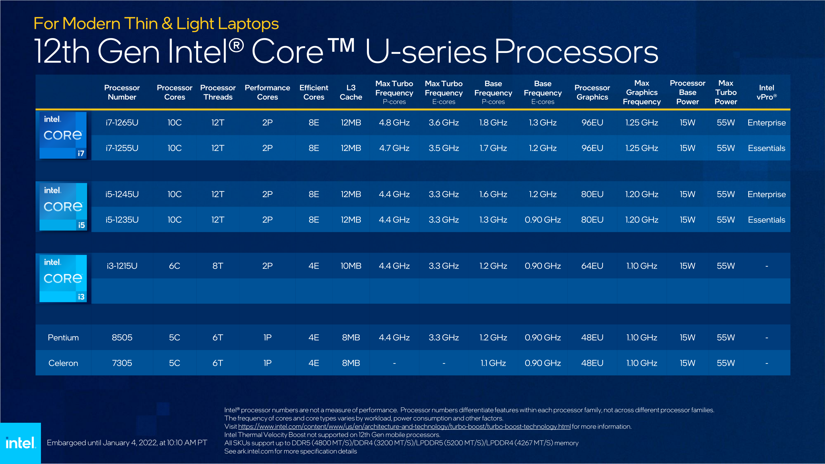
| Intel 12th Gen Core-U at 15 W (UP3) | ||||||||
| AnandTech | Core P+E |
Base E |
Turbo E |
Base P |
Turbo P |
GFX EUs |
GPU MHz |
L3 MB |
| i7-1265U | 2+8 | 1300 | 3600 | 1800 | 4800 | 96 | 1250 | 12 |
| i7-1255U | 2+8 | 1200 | 3500 | 1700 | 4700 | 96 | 1250 | 12 |
| i5-1245U | 2+8 | 1200 | 3300 | 1600 | 4400 | 80 | 1200 | 12 |
| i5-1235U | 2+8 | 900 | 3300 | 1300 | 4400 | 80 | 1200 | 12 |
| i3-1215U | 2+4 | 900 | 3300 | 1200 | 4400 | 64 | 1100 | 10 |
| Pentium 8505 | 1+4 | 900 | 3300 | 1200 | 4400 | 48 | 1100 | 8 |
| Celeron 7305 | 1+4 | 900 | N/A | 1100 | N/A | 48 | 1100 | 8 |
If the transition from P to U wasn’t a giveaway that we’re coming down the stack, Intel also makes this distinction by putting a 5 as the last digit in every processor. That’s because the 0 parts are the even lower 9 W hardware we’ll cover a bit further down.
The top line Core i7-U at 15 W comprises two processors, each with two performance cores and eight efficiency cores, with the Core i7-1265U having a turbo up to 4.8 GHz. Both parts have 96 execution units for graphics running at up to 1.25 GHz, which is slightly slower than the P series. But the power range is listed as 15 W on base and 55 W on turbo. Ultimately this isn’t a massive difference from the P-series in all honesty, as at the top end the U series is only 9 W less for the loss of four performance cores.
Mid-range Core i5-U at 15 W has the same i7-to-i5 reduction we saw in the P-series. We still get two performance cores and eight efficiency cores, but the integrated graphics come down from 96 to 80 execution units. The power range of 15-55W is still the same.
Now at the low end is where we get interesting. There is a single Core i3, running in a 2+4 configuration with 64 execution units, but it’s the Pentium and Celeron that are worth looking at. Both the Pentium 8505 and Celeron 7305 (notice there’s no U) run with only a single performance core, four efficiency cores, and 48 execution units on graphics. In our lists, Intel has the Pentium with turbo frequencies up to 4.4 GHz, while the Celeron continues to not get any kind of turbo boost ability. What we end up with is a 5 core configuration.
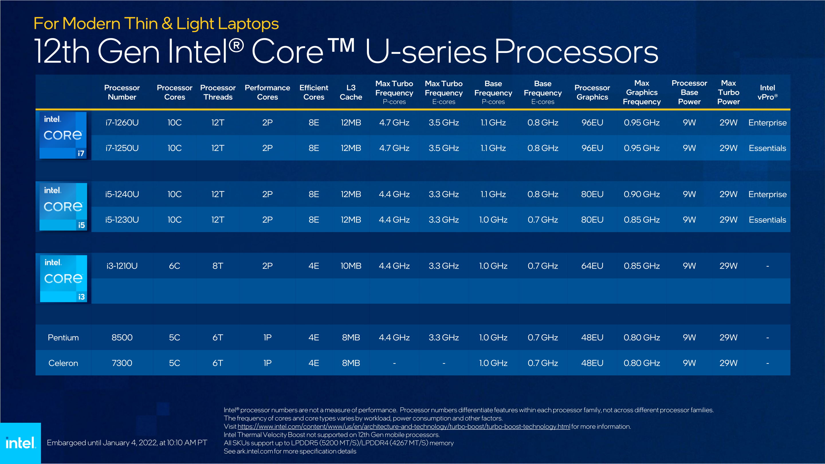
| Intel 12th Gen Core-U at 9 W (UP4) | ||||||||
| AnandTech | Core P+E |
Base E |
Turbo E |
Base P |
Turbo P |
GFX EUs |
GPU MHz |
L3 MB |
| i7-1260U | 2+8 | 800 | 3500 | 1100 | 4700 | 96 | 950 | 12 |
| i7-1250U | 2+8 | 800 | 3500 | 1100 | 4700 | 96 | 950 | 12 |
| i5-1240U | 2+8 | 800 | 3300 | 1100 | 4400 | 80 | 900 | 12 |
| i5-1230U | 2+8 | 700 | 3300 | 1000 | 4400 | 80 | 850 | 12 |
| i3-1210U | 2+4 | 700 | 3300 | 1000 | 4400 | 64 | 850 | 10 |
| Pentium 8500 | 1+4 | 700 | 3300 | 1000 | 4400 | 48 | 800 | 8 |
| Celeron 7300 | 1+4 | 700 | N/A | 1000 | N/A | 48 | 800 | 8 |
Funnily enough, when we move to the 9 W family of hardware, not a lot changes, each configuration still has the same core count as the 15 W version, although in each case the base frequencies are lower. These 9 W processors also only have a maximum turbo power consumption of 29 W. It is worth pointing out that even though the two i7s look identical, the top i7 supports vPro Enterprise, while the other only supports vPro Essentials. The same delineation exists for the Core i5 parts as well.
Between the three families, there are some other differences.
The 9 W processors support both LPDDR4-4267 and LPDDR5-5200, whereas the 15W and 28 W processors support those as well as DDR4-3200 and DDR5-4800. Usually support for DDR means double the peak memory capacity available, leading to 128 GB on DDR4/DDR5 and only 64 GB on LPDDR4/LPDDR5.
The 28 W processors also have Turbo Boost Max 3.0, which is Intel’s marketing name for favored core. It means that one of the cores on the P-series Core i7 is designated the ‘best’ core, and can turbo up higher than the others, typically +100 MHz or +200 MHz, depending on the configuration. This would push the Core i7-1280P from 4.8 GHz to 5.0 GHz, and I’d check on Intel’s official ark.intel.com database for the details, but despite the link being in the slide deck, the public database has not yet been updated.
Other details are TBD, given that Intel has not provided full breakdowns of the chipset and PCIe support for anything other than the H-series processors at this time. This is despite Intel’s own press release for CES states that U-Series and P-Series design wins will available in the first quarter, Evo-enabled designs will come in the first half of the year, ‘including foldables, 2-in-1s, detachables, and others’.
With AMD pushing its 15 W parts more into the 28 W space stating that it has made a breakthrough in its power gating design, it’s interesting to see that instead Intel has extended its 45 W processor down to 28 W. It’s going to be very confusing for customers to understand what’s in their product for sure, but not only that, it’s going to be interesting to see how OEMs deal with a CPU market that is becoming more fractured when it comes to performance, functionality, power, and design. Meanwhile, there are some shortages going on relating to display controllers and other similar things, causing schedules to slip or portfolios to adjust accordingly.


91 Comments
View All Comments
Spunjji - Friday, January 21, 2022 - link
Indeed - they've been disabling turbo for no obvious reason besides punishing cash-strapped customers for a while now, but it's rare to see them do it when the clocks are already in the toiletnewblar - Thursday, January 20, 2022 - link
If not for pricing the 9 watt U parts would be good for ipad m1 android equivalent tablets. Also now with an engineer ceo again I feel like they could engineer a competitive soc for smartphones considering qualcomms struggles.abufrejoval - Thursday, January 20, 2022 - link
All this binning and salvaging used to be meaningful: With the advent or multi-core chips, selling partial defects e.g. with 3 out of 4 cores still good, not only made a lot of sense, it also made me feel quite warm and comfy about those handicapped chips finding a less demanding home than mine.But when I look at this plethora of chips and the nature of fabbing, it’s obviously quite impossible to achieve such consistent defect patterns across so many process generations, were always some cores or parts of the cache and iGPU either wind up defective or exceeding voltage threshold, which requires culling of cores, cache or GPU blocks in the name of TDP.
Significant engineering talent is obviously dedicated at producing sub-par parts from excellent chippery and I wonder what the psychological toll is on those poor bastards, who were made responsible for i3 or Pentium parts. Imagine them going to bed every night, hoping that one day they might be permitted to do i7, i9, i11 or i13! It’s just heart wrenching!
Sure, the original Pentium was a hothead and tended to unsolder itself, but it also set Intel apart from all 80486: How did it become a banner of shame? Ok, I’m drifting...
I am quite literally just fed up with Intel: too many choices, none satisfying. What I want is the ability to balance compute power versus noise and battery capacity, so just sell me a chip and levers which allow me to slide the bars between 5 and 45 Watts for a mobile and a NUC, 35 to 250 Watts on desktop, and let me adjust P1, P2 and max fan speed according to my current need at run-time.
Then I might want to order slices of P or E for my silicon pizza and that’s it!
Everything else is just torture designed to push me to i-max, which currently leads me to buy full chunks of AMD APUs or CCDs, from 15 to 150 Watts in my home lab, plenty more in the DC.
Spunjji - Friday, January 21, 2022 - link
"How did it become a banner of shame"They needed to get some distance from all those years of pushing expensive Netburst chips on people, lying about how good it was, and paying OEMs not to stock competitor parts.
Mike Bruzzone - Friday, January 21, 2022 - link
abufrejoval, Thank you for these astute observations on falling out on sort. Under Docket 9341 consent order disabling good parts is monitored and essentially not permitted as anticompetitive to target others with down bin parts that did not fall out of sort organically. At the same time unlike Ivy when the Intel practice of disablement at Intel became pervasive, by Comet, the cost became prohibitive on a full cores mask set design. The same is true with TSMC Zen octa high cost of disablement v. organic fall out. Intel has moved to dice area optimized masks which AMD is just beginning to do with 65/64xx Goby. The marginal cost to sort for Alder Lake Pentiums and Celeron is approximately $5 per component that have approximately a $15 all up production cost. Intel relies on statistical modeling to analyze projectable yield and the process is very sophisticated in actual use. mbabufrejoval - Saturday, January 22, 2022 - link
Thanks Mike for the reference, (https://www.ftc.gov/sites/default/files/documents/... which I've just read through.Here my naïve self had not been aware how the FTC had managed to head off the most egregious abuses, countered in gory detail in that document: I wonder if the document has been updated since, and what it should look like today.
But I can’t see any reference to intentionally disabled chips in there… is that perhaps in an updated document or is that simply a different number?
Anyhow, it fully explains how Intel wants to go back to feature licensing on their chips, because it completely avoids such a “do not fuse off working parts” decree, which obviously hasn’t been illegal in the mainframe world. Once they’re sure they didn’t botch the implementation (like currently the base overclock with the AL non-K parts), they’d certainly want to use that mechanism to squeeze their customers.
And to be honest, it wouldn’t be all bad, if it wasn’t then abused later. But I’m sure they’d become extremely creative, once it suits them.
Among the things I’d consider fair would be the ability to add and extract core/ECC/iGPU/clock unlocking codes from a SoC and resell them, consumer to consumer. So, if grandpop passed on his surfing machine to his granddaughter, she can turn it into a modest gaming rig buying somebody else’s unlock code off eBay. Sure, it could be tied to a generation, as long as they don’t increment those artificially to below a true technical cadence just to kick this out again.
Since these are purely digital assets, Intel shouldn’t be allowed to raise their prices through the roof three years later, just because they want to sell new chips.
Somebody better start planning a global rule book there, before it takes another ten years to pass the dozen different anti-competitive bodies to react.
On the economical side, selling octa-core chunks as a reduced performance dual-cores like IBM does for mainframes, can’t be fully repeated in PCs or consoles, I guess. With Intel having their own fab in theory their ability to switch wafers between M, X, XXXL or any other die variant on short term, give them a huge advantage vis-à-vis an AMD that has to wait in line at TMSC. But that only lasts as long as AMD/TMSC can’t cook up better post-fab/packaging stage modularity, which the 3D cache stack is hinting at, vs. Foveros etc. The CCD/IOD combo certainly stirred some engineering into action.
As a fan of good engineering I am very much looking forward to the solutions both sides with think up there.
But then come the bean-counters and that's where I am much less hopeful. With Charly warning against Pluton malware on AMD and Intel seemingly trying to leap ahead of AMD everywhere, all this doesn’t look like consumers will be served better with something they can use longer, which is the only progress I am really interested in.
Mike Bruzzone - Monday, January 24, 2022 - link
I’m enlisted by the FTC to monitor Docket 9341 consent agreement since 2010; AMD, Intel, Nvidia and Via, contracted by USDOJ to recover Intel Inside price fix for buyer return.No (hidden) Reference to “intentionally disabled chips”, FTC is amorphous in determinations.
Premeditated disablement of a good hexa to produce a quad or quad to produce a dual and for the specific purpose of flooding channel to limit competitive participation ‘organically’ falls under “no efficiency justification” and “raising cost” which is a Sherman Act Section 2 violation where Intel Inside rebate falls under Section 1 combining contracts “raising costs” as EUCC 37.990 described “unnecessary avoidable cost charge”.
FTC mandate pursuant disablement falls generally within 9341 consent agreement “Part IV A; respondent shall not invite, enter into, implement, continue, enforce any condition, policy, practice, agreement, contract, understanding, or any requirement . . .” Note, pursuant any OEM full line procurement the amount of down bin product is specified in the Intel OEM / IDM purchase agreement. Down bin is often freebie ‘sales close incentive’ Intel throws to any sales contract and specified for OEM/IDM 'supply chain' production planning.
The practice of disablement “raising cost” generally falls under Price < Cost and in this case on the cost of additional production steps associated disablement from good too bad to meet a contract supply obligation vis-à-vis what might organically fall out of sort.
Thank you for the mainframe world observation “licensing features” applied to Intel; aha!
On the AL non-K OC BIOS mod, Intel has done this before at risk production to goose sales out of the gate and then claims ignorance and no warranty responsibility; a spring board sales accelerator for certain end customer types that would not otherwise have purchases a K part.
On Intel locking out CPU upgrade I thought it prevented down grade i5 to i3 but not upgrade i5 to i7. Either way I do not believe in disabling features including Nvidia HLR on aftermarket value effect and unseen consequences into future essentially over segmentation or lock out.
EUCC traditionally leads in defining the rule book. I’m actually retained by Congress where once the FTC completes a project tends not to mind it. I do submit rule changes to Congress.
True, PC’s don’t have the IBM OLTP mark up; selling octa at reduced performance; enabling only two cores abd a lot of cache for databases. Note Epyc can be characterized and its CCX and L3 partitioned like a ‘many instances” GPU but AMD does not talk about it outside a clutch of developers.
Quad Scalable from Intel low core count deca can also be characterized (or disabled) as a quad for maximum L3 per core so it does happen in the high cost : price / margin systems market.
Intel coming out of its sabotage post Comet revitalized its mask shop at Tiger lake quad for die size optimized mask set. AMD with cash again started at GPU Beige Goby where in relation Intel AMD has to go to 3rd party mask cost.
Thanks for your thoughts.
I too look to enterprise serving customers on responsibilities in technocracy "meet the needs of customers and society as cost effectively as possible", stewardship cognizant welfare", "complimentary participation, partnership, cost and reward sharing", planning for an adequate economic return on investment", "steward in the countries of industry operation", "sustainable growth models that make economic sense", Watson Jr.
mb
ChrisGX - Saturday, January 22, 2022 - link
...too many choices, none satisfying.Yes, that could easily be the epitaph on Intel's tombstone.
ChrisGX - Thursday, January 20, 2022 - link
Apple, I believe, offers one chip to satisfy all of the use cases covered by this long list of chips. It is called the M1. If Intel was serious about consumer needs it would stop playing the pointless market segmentation game -- it is all sound and fury signifying nothing.If Intel was doing right by consumers it would cover all of these use cases with two chips -- one competitive with the M1 and another non-premium part that is cheaper and more energy efficient that is suited to users who don't need the premium option.
KPOM - Thursday, January 20, 2022 - link
To be fair, they have the M1, 3 variants of the M1 Pro (8/14 Core CPU/GPU, 10/14, 10/16) and 2 variants of the M1 Max (10/24, 10/32), so they have 6 chips, which is still much fewer than 20.