Original Link: https://www.anandtech.com/show/13186/flash-memory-summit-2018-yangtze-memory-technology-keynote-live-blog-unleashing-3d-nand
Flash Memory Summit 2018, Yangtze Memory Technology Keynote Live Blog: Unleashing 3D NAND
by Ian Cutress & Billy Tallis on August 7, 2018 5:50 PM EST
05:53PM EDT - The final talk of this session is from Yangtze Memory Technology (YMTC). We published their announcement this week, but they have set a very interesting talk for the show. The talk is called 'Unleasing 3D NAND's Potential with an Innovative Architecture'.
05:54PM EDT - Set to start in 10 minutes!
05:55PM EDT - Here is our news from earlier in the week:
05:55PM EDT - https://www.anandtech.com/show/13166/yangtze-memory-unveils-xtacking-architecture-for-3d-nand-up-to-3-gbps-io
05:57PM EDT - YMTC is a newcomer to FMS, and they seem to have grabbed Samsung's vacated time slot
06:03PM EDT - OK here we go
06:03PM EDT - Simon Yang to the stage
06:03PM EDT - CEO
06:04PM EDT - 'We're a new kid in the neighbourhood'
06:04PM EDT - Usually Yang is at IEDM
06:04PM EDT - A couple of years ago, he knew next to nothing about NAND
06:05PM EDT - 'we are a bunch of good kids
06:05PM EDT - Make a contribution to the industry
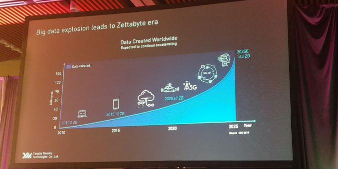
06:06PM EDT - Expected 163 ZB Big Data explosion by 20205
06:06PM EDT - Most data is garbage
06:06PM EDT - But our habit is to store data
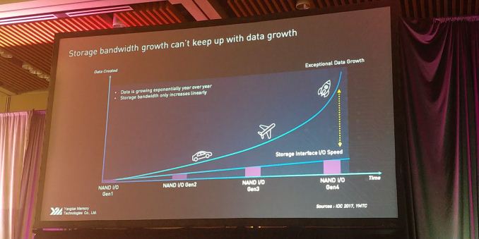
06:07PM EDT - Data speed only increasing linearly, but data created is exponential
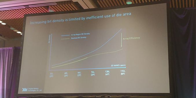
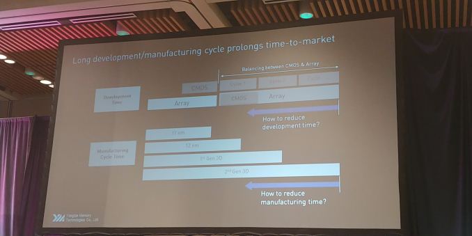
06:07PM EDT - Challenges of NAND: I/O speed, bit density, and time to market
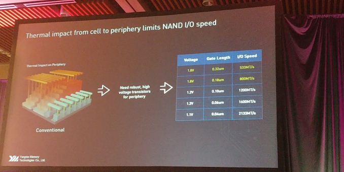
06:09PM EDT - Thermal impact limits the scaling and speed of NAND
06:09PM EDT - High thermal process prevents scaling of process
06:09PM EDT - (They just turned the lights on, so can't get good photos)
06:10PM EDT - Manufacturing cycle times have been getting longer
06:10PM EDT - YMTC aim to solve these problems
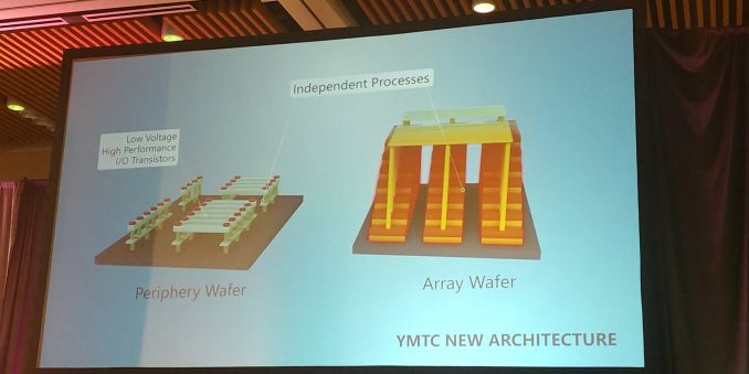
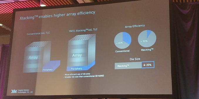
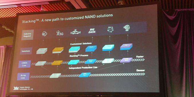
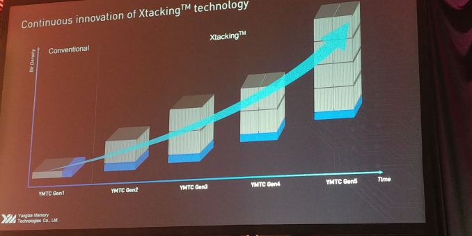
06:10PM EDT - Solution is Xtacking
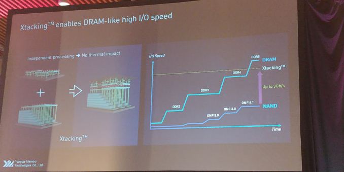
06:11PM EDT - Using low voltage periphery transistors and stacking allows for faster IO
06:12PM EDT - Moves IO speed up to DDR speeds
06:12PM EDT - Up to 3 Gbps IO
06:12PM EDT - Use up to 14nm to boost IO speed
06:12PM EDT - Putting the periphery above the stack
06:13PM EDT - YMTC proposes 3Gbps wheil Samsung and SK Hynix are talking 1.4Gbps and 1.2Gbps
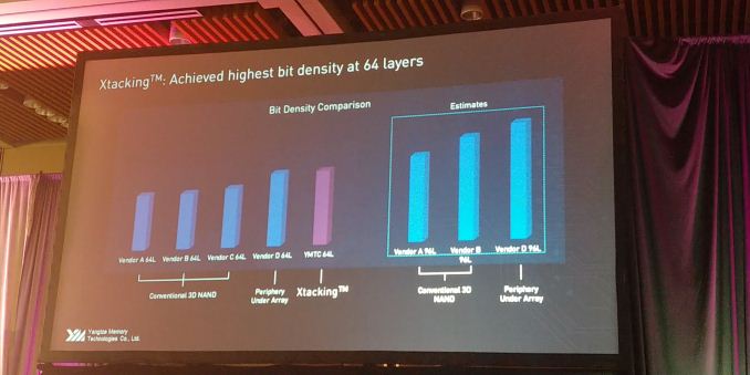
06:13PM EDT - Bit density on YMTC 64-layer only 10-20% below 96 layer
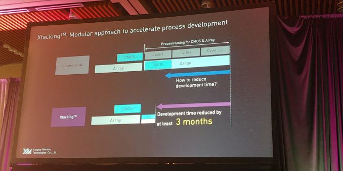
06:14PM EDT - reducing time to market by 3 months
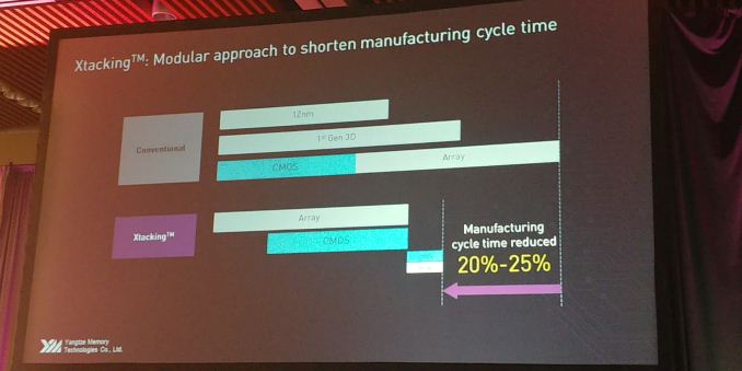
06:14PM EDT - develop wafers differently means can work on independently, and shorten manufacturing cycle time by 20-25%
06:14PM EDT - Also allows for customized designs for each market
06:15PM EDT - Use different peripheral logic for each customer
06:15PM EDT - Allowing customers to win
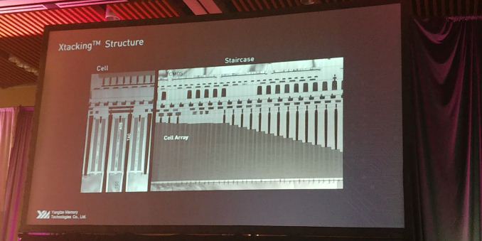
06:15PM EDT - Cells and staircase structure
06:16PM EDT - Pushing the technology into low nanometer generations
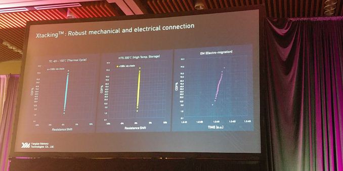
06:16PM EDT - Re-engineering the interface material
06:16PM EDT - Re-engineering based on design rules for each wafer
06:16PM EDT - Develop own slurry to enable the technology
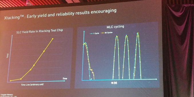
06:17PM EDT - SLC yield rate is increasing, MLC cycling is getting better
06:17PM EDT - Yield is not Xtacking limited
06:17PM EDT - Working on multiple generations simultaneously
06:18PM EDT - YMTC wants to contribute to the industry
06:18PM EDT - The main question is where di YMTC come from
06:18PM EDT - Story time
06:18PM EDT - Yang previously worked for Intel
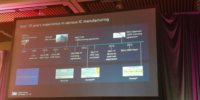
06:19PM EDT - Then toured around the world, then worked for 12-inch fab in 2012
06:19PM EDT - Ended up in XMC
06:19PM EDT - This is where Xtacking happens
06:19PM EDT - Mainly NOR up to now
06:20PM EDT - 2015, signed joint 3D NAND agreement with Spansion
06:20PM EDT - Working on wafer level stacking technology
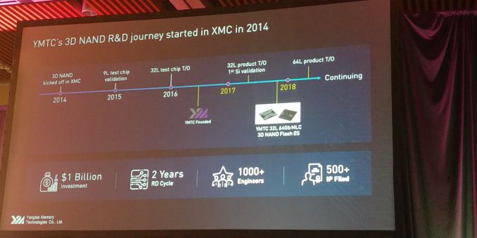
06:20PM EDT - 3D NAND R&D started in 2014
06:21PM EDT - $1B development in 3D NAND
06:21PM EDT - YMTC founded in 2016
06:21PM EDT - YMTC founded in 2016
06:21PM EDT - hiring lots of people to catch up to incumbants
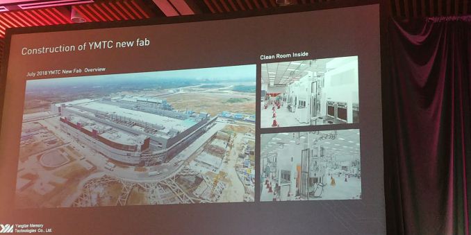
06:22PM EDT - Fab is 60-70k sq m
06:22PM EDT - First gen product currently made in small fab
06:22PM EDT - New fab will mainly be focused on the next generations
06:23PM EDT - YMTC is a group with pretty good tech capability for development
06:23PM EDT - Not afraid to go down new paths
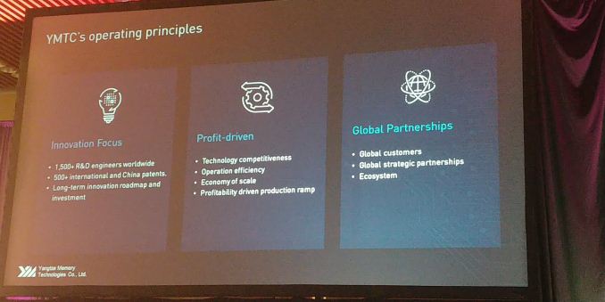
06:23PM EDT - Follow market rule, and very much profit driven
06:23PM EDT - First gen product is already in very high yield
06:23PM EDT - But not in volume ramp, because from cost perspective it is not competitive
06:24PM EDT - Only want to ramp when it is cost competitive
06:24PM EDT - Very open for collaboration
06:24PM EDT - (most other 32L 3D NAND designs were also not very cost competitive)
06:24PM EDT - Want to serve the whole global market
06:24PM EDT - That's a wrap. Interesting stuff. Now meetings for the rest of the day

