AMD Kaveri Review: A8-7600 and A10-7850K Tested
by Ian Cutress & Rahul Garg on January 14, 2014 8:00 AM ESTA Deep Dive on HSA
For our look into Heterogeneous System Architecture (HSA), Heterogeneous Unified Memory Architecture (hUMA) and Heterogeneous Queuing (hQ), our resident compute expert Rahul Garg steps up to the plate to discuss the implication, implementation and application of such concepts:
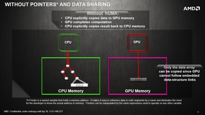
GPUs are designed for solving highly parallel problems - for example, operations on matrices are highly parallel and usually well-suited to GPUs. However, not every parallel problem is suitable for GPU compute. Currently using GPUs for most problems requires copying data between the CPU and GPU - for discrete GPUs, typically an application will copy data from system RAM to the GPU memory over the PCIe bus, do some computation and then send the results back over the PCIe bus when the computation is complete. For example, matrix addition is a highly parallel operation that has been well documented and optimized for parallelism on CPUs and GPUs alike, but depending on the structure of the rest of the application, may not be suitable for GPU acceleration if the copy demands over the PCIe bus are strenuous to the overall speed of the application. In this example, the data transfer time alone will often be more expensive than doing the matrix addition on the CPU. The data copy between the CPU and the GPU also introduces complexity in software development.
There are two reasons for the necessity of fast data transfer today. First, GPU compute currently usually implies using a discrete GPU attached to the system over the PCIe bus. Discrete GPUs have their own onboard RAM, usually in the range of 1GB to 4GB or up to 12GB on some recent server-oriented cards. The onboard RAM may have a high bandwidth (say GDDR5) in order to hide latency between thread context switching, sometimes cited as the holy-grail in high memory access compute tasks. In this setup, even if we assume that the GPU could read/write data in system RAM over PCIe bus, it is often more efficient to just transfer all relevant data to this onboard RAM once only, and let the compute kernels read/write data from the onboard GPU RAM instead of attempting to read/write data slowly over PCIe. The second reason for data copies is that the CPU and the GPU have distinct address spaces. Before HSA, they could not make sense of each other's address spaces. Even integrated GPUs, which do physically share the same memory, did not have the necessary bookkeeping machinery necessary for a unified address space. HSA addresses this second scenario.
People have been trying many techniques to avoid the data transfer overhead. For example, you can try to do data transfers in parallel with some other computation on the CPU so that computation and communication overlap. In some cases, the CPU can be bypassed altogether, for example by transferring some file data from a PCIe SSD directly to the GPU using GPUDirect. However, such techniques are not always applicable and require a lot of effort from the programmer. Ultimately, true shared memory between CPU and GPU is the way to go for many problems though discrete GPUs with their onboard high-bandwidth RAM will shine on many other problems despite the data-copy overhead.
Unified memory: State of the art before HSA
The terms "shared memory" or "unified memory" are actually thrown about quite frequently in the industry and can mean different things in different contexts. We examine the current state of art across platform distributors:
NVIDIA has introduced "unified memory" in CUDA. However, on current chips, it is a software-based solution that is more of a convenience for software developers and hidden behind APIs for ease of use. The price of data transfer still needs to be paid in terms of performance, and NVIDIA's tools merely hide some of the software complexity. However, NVIDIA is expected to offer true shared memory in the Maxwell generation, which will likely be integrated into the successor of Tegra K1 in 2015 or 2016.
AMD: AMD touts "zero copy" on Llano and Trinity for OpenCL programs. However, in most cases, this only provides a fast way to copy data from CPU to GPU and the ability to read data back from GPU in some limited cases. In practice, the zero copy feature has limited uses due to various constraints such as high initialization cost. For most use cases, you will end up copying data between CPU and GPU.
Intel: Intel provides some support for shared memory today on the Gen7 graphics in Ivy Bridge and Haswell exposed through OpenCL and DirectX. Intel's CPU/GPU integration is actually more impressive than Llano or Trinity from the perspective of memory sharing. However, sharing is still limited to some simple cases as it is missing pointer sharing, demand-based paging and true coherence offered in HSA and thus the integration is far behind Kaveri. I am expecting better support in Broadwell and Skylake. Intel's socketed Knights Landing (future Xeon Phi) product may also enable heterogeneous systems where both CPU and accelerator access the same memory, which might be the way forward for discrete GPUs as well (if possible).
Others: Companies like ARM, Imagination Technologies, Samsung and Qualcomm are also HSA Foundation members and probably working on similar solutions. Mali T600 and T700 GPUs expose some ability of sharing GPU buffers between CPU and GPU through OpenCL 1.1. However, I don't think we will see a full HSA stack from vendors other than AMD in the near future.
As of today, HSA model implemented in Kaveri is the most advanced CPU-GPU integration yet and offers the most complete solution of the bunch.
hUMA: Unified Memory in HSA
Now we examine the unified memory capabilities provided in HSA. The main benefits of having a heterogeneous unified memory architecture in HSA boil down to the addressable memory space. By reducing the cost of having the CPU and GPU access the same data, compute can be improved or offloaded without worrying about the expense of such an operation.
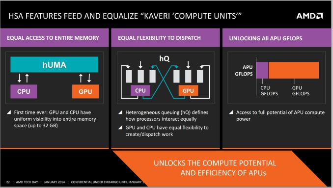
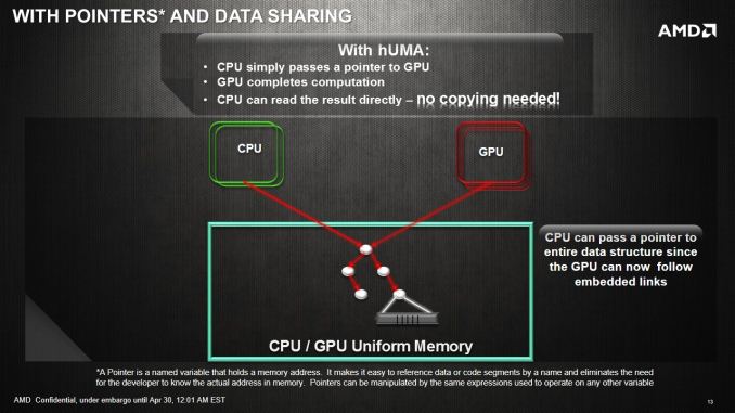
Eliminating CPU-GPU data copies: GPU can now access the entire CPU address space without any copies. Consider our matrix addition example again. In an HSA system, the copy of input data to GPU and copy of results back to CPU can be eliminated.
Access to entire address space: In addition to the performance benefit of eliminating copies, the GPU is also no longer limited to the onboard RAM as is usually the case with discrete GPUs. Even top-end discrete cards top out at about 12GB of onboard RAM currently while a CPU had the advantage of having access to potentially a much larger pool of memory. In many cases, such as scientific simulations, this would mean that the GPU can now work on much larger datasets without any special effort on the part of the programmer to somehow fit the data into GPU's limited address space. Kaveri will have access up to 32GB DDR3 memory, whereby the limiting factor is more the lack of 16GB unregistered non-ECC memory sticks on the market. The latency between the APU and the DRAM still exists however, meaning that a large L3 or eDRAM in the future might improve the scenario, especially in memory bandwidth limited scenarios and pre-empting data fetching.
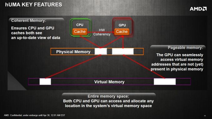
Unified addressing in hardware: This is the big new piece in Kaveri and HSA that is not offered by any other system currently. Application programs allocate memory in a virtual CPU memory space and the OS maintains a mapping between virtual and physical addresses. When the CPU encounters a load instruction, it converts the virtual address to physical address and may need the assistance of the OS. The GPU also has its own virtual address space and previously did not understand anything about the CPU's address space. In the previous generation of unified memory systems like Ivy Bridge, the application had to ask the GPU driver to allocate a GPU page table for a given range of CPU virtual addresses. This worked for simple data structures like arrays, but did not work for more complicated structures. Initialization of the GPU page table also created some additional performance overhead.
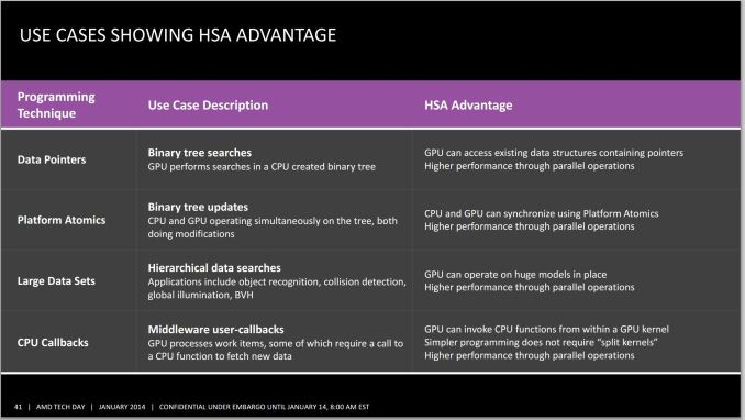
In HSA, the GPU can directly load/store from CPU virtual address space. Thus, the application can directly pass CPU pointers enabling a much broader class of applications to take advantage of GPU. For example, sharing linked-lists and other pointer-based data structures is now possible without complicated hijinks from the application. There is also no driver overhead in sharing pointers, and thus provides better efficiency.
With this solution, the CPU and the GPU can access the same data set at the same time, and also perform work on the data set together. This enables developers to program for high utilization scenarios, and gets around AMD’s calculations of 800+ GFLOPs coming from a single Kaveri APU. With up to 12 compute cores, despite having to use CPU and GPU compute cores differently and with different kernels, they can at least all access the same data with zero overhead. It will still be up to the developer to manage locks and thread fences to ensure data coherency.
Demand-driven paging: We overlooked one detail in the previous discussion. Converting virtual addresses to physical addresses is a non-trivial task - the page containing the desired physical location may not actually be in memory and may need to loaded from, say, the disk and requires OS intervention. This is called demand-driven paging. GPUs prior to Kaveri did not implement demand-driven paging. Instead, the application had to know in advance what range of memory addresses it was going to access and map those to a GPU buffer object. The GPU driver then locked the corresponding pages in memory. However, in many cases the application programmer may not know the access pattern beforehand. Pointer-based data structures like linked lists, where the nodes may be pointing to anywhere in memory, were difficult to deal with. Demand-driven paging, together with unified addressing, allows sharing of arbitrary data structures between CPU and GPU and thus opens the door to GPU acceleration of many more applications.
CPU-GPU coherence: So far we have discussed how the GPU can read/write from the CPU address space without any data copies. However, that is not the full story. CPU and the GPU may want to work together on a given problem. For some types of problems, it is critical that the CPU/GPU be able to see each other's writes during the computation. This is non-trivial because of issues such as caches. HSA memory model provides optional coherence between the CPU and the GPU through what is called acquire-release type memory instructions. However, this coherence comes at a performance cost and thus HSA provides mechanisms for the programmer to express when CPU/GPU coherence is not required. Apart from coherent memory instructions, HSA also provides atomic instructions that allow the CPU to GPU to read/write atomically from a given memory location. These ‘platform atomics’ are designed to do as regular atomics, i.e. provide a read-modify-write operation in a single instruction without developing custom fences or locks around the data element or data set.
HSAIL: Portable Pseudo-ISA for Heterogeneous Compute
The HSA Foundation wants that the same heterogeneous compute applications run on all HSA-enabled systems. Thus, they needed to standardize the software interface supported by any HSA-enabled system. HSA foundation wanted a low-level API to the hardware that can be targeted by compilers of different languages. Typically compilers target the instruction-set of a processor. However, given the diversity of hardware being targeted by HSA (CPUs, GPUs, DSPs and more), standardizing on an instruction-set was not possible. Instead, HSA Foundation has standardized on a pseudo-instruction set called HSAIL. HSAIL stands for HSA Intermediate Language. The idea is that the compiler for a high-level language (like OpenCL, C++ AMP or Java) will generate HSAIL and the HSA driver will generate the actual binary code using just-in-time compilation. The idea of a pseudo-ISA has been used in many previous portable technologies such as Java bytecode and the Direct3D bytecode. HSAIL is low-level enough to expose many details of the hardware and has been carefully designed such that the conversion from HSAIL to binary code can be very fast.
In terms of competition, Nvidia provides PTX which has similar goals to HSAIL in terms of providing a pseudo instruction set target for compilers. PTX is only meant for Nvidia systems, though some research projects do provide alternate backends such as x86 CPUs. HSAIL will be portable to any GPU, CPU or DSP that implements HSA APIs.
hQ: Optimized Task Queuing in HSA
Heterogeneous Queuing is an odd term for those not in the know. What we have here is a series of code that calls upon another function during its processing, one which requires the performance of another device. Say for example I am running a mathematical solver, and part of the code that runs on the GPU requires CPU assistance in computing. The way the threads are handled is coined ‘heterogeneous queuing’. HSA brings three new capabilities in this context to Kaveri and other HSA systems compared to previous-gen APUs.
User-mode queuing: In most GPGPU APIs, the CPU queues jobs/kernels for the GPU to execute. This queuing goes through the GPU driver and requires some system calls. However, in HSA the queuing can be done in user-mode which will reduce the overhead of job dispatch. The lower-latency of dispatch will make it feasible to efficiently queue even relatively small jobs to the GPU.
Dynamic parallelism: Typically the CPU queues work for the GPU but the GPU could not enqueue work for itself. NVIDIA introduced the capability for GPU kernels to call other GPU kernels with the GK110/Titan and named this dynamic parallelism. HSA systems will include dynamic parallelism.
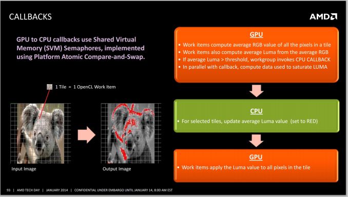
CPU callbacks: With Kaveri, not only will the GPU be able to queue work for itself, it will be able to queue CPU callback functions. This capability goes beyond competitor offerings. CPU callbacks are quite useful in many situations, for example CPU callbacks maybe required to call system APIs that cannot run on the GPU, legacy CPU code that has not yet been ported to the GPU or may simply be code that is more complex, and thus suitable on the CPU.
Programming Tools Roadmap
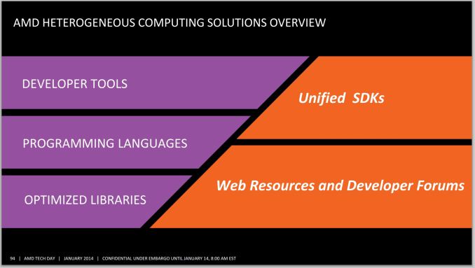
Given that many users write in different languages for many different purposes, AMD has to have a multifaceted approach when it comes to providing programming tools.
Now we examine part of the software roadmap for programming tools for HSA:
Base HSA stack: Base HSA execution stack supporting HSAIL and HSA runtime for Kaveri is expected to become available in Q2 2014.
LLVM: HSAIL is only one piece of the puzzle. While many compiler writers are perfectly happy to directly generate HSAIL from their compilers, many new compilers today are built on top of toolkits like LLVM. AMD will also open-source an HSAIL code generator for LLVM, which will allow compiler vendors using LLVM to generate HSAIL with very little effort. So we may eventually see compilers for languages such as C++, Python or Julia targeting HSA based systems at some point. Along with the work being done in Clang to support OpenCL, the LLVM to HSAIL generator will also simplify the work of building OpenCL drivers for HSA-based systems. In terms of competition, NVIDIA already provides a PTX backend for LLVM.
OpenCL: At the time of launch, Kaveri will be shipping with OpenCL 1.2 implementation. My understanding is that the launch drivers are not providing HSA execution stack and the OpenCL functionality is built on top of their legacy graphics stack built on top of AMDIL. In Q2 2014, a preview driver providing OpenCL 1.2 with some unified memory extensions from OpenCL 2.0 built on top of HSA infrastructure should be released. A driver with support for OpenCL 2.0 built on top of HSA infrastructure is expected in Q1 2015.
C++ AMP: C++ AMP was pioneered by Microsoft and the Microsoft stack is built on top of DirectCompute. DirectCompute does not really expose unified memory, and even Direct3D 11.2 only takes only preliminary steps towards unified memory. Microsoft's C++ AMP implementation targets DirectCompute and thus won't be able to take full advantage of features offered by HSA enabled systems. However, C++ AMP is an open specification and other compiler vendors can write C++ AMP compilers. HSA Foundation member Multicoreware is working with AMD on providing a C++ AMP compiler that generates HSAIL for HSA enabled platforms, and OpenCL SPIR for other platforms (such as Intel).
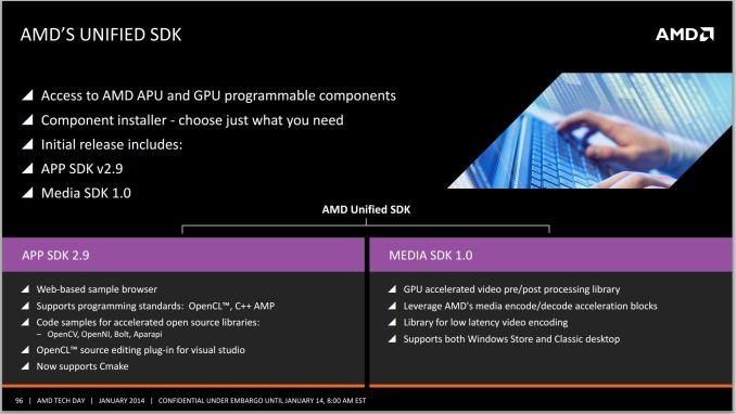
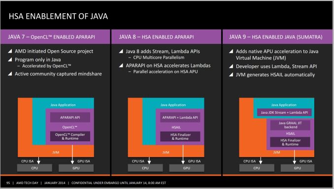
Java "Sumatra" and Aparapi: AMD already provides an API called Aparapi that compiles annotated Java code to OpenCL. AMD will be updating Aparapi to take advantage of HSA in Java 8 and it will be ready sometime in 2014. In addition, Oracle (owner of Java) also announced a plan to target HSA by generating HSAIL from Java bytecode in their HotSpot VM. This is expected to be released with Java 9 sometime in 2015. It will be interesting to watch if IBM, which has announced a partnership with NVIDIA, will also enable HSA backends in its own JVM.
HSA Conclusion
Overall, HSA brings many new capabilities compared to the basic GPGPU compute of AMD platforms to this point. Unified memory in HSA is an extremely exciting step due to the explicit elimination of data-copies, the ability for the GPU to address large amounts of memory and the sharing of complex data structures will enable heterogeneous computing for many more problems. Ability for the GPU to queue kernels for itself, or even do CPU callbacks are both great additions as well. CPU/GPU integration in HSA is definitely a step above the competition and does have the potential of making them more equal peers than the current model. As a compiler writer, I do think that HSA systems will be easier to program for both compiler writers as well as application developers and in the long term does have the potential of making heterogeneous computing more mainstream.
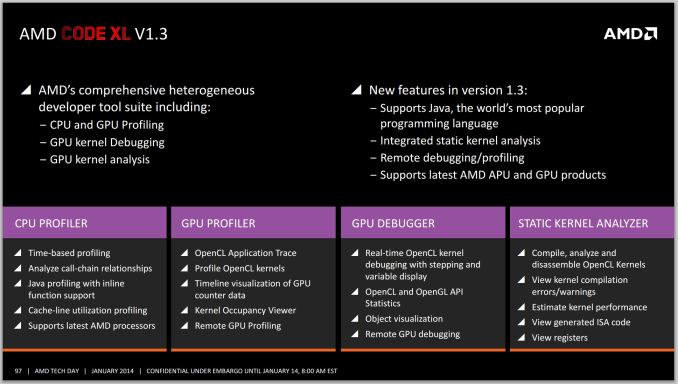
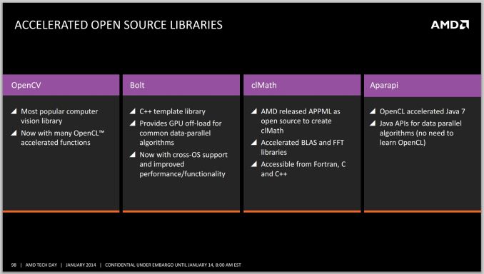
However, HSA will only begin delivering when the software ecosystem takes advantage of HSA capabilities, and this will not happen overnight. While HSA is impressive at the architecture level, AMD also needs to deliver on its software commitments as soon as possible. This not only includes HSA enabled drivers, but also tools such as profilers and debuggers, good documentation and other pieces such as the LLVM backend. I would also like to see more projects for programming languages compiling to HSA, especially open source libraries which AMD are working on for their HSA implementation.
Finally, whether HSA succeeds or fails will also depend upon what direction HSA Foundation members such as Qualcomm, ARM, TI, Imagination tech and Samsung take. At this point, no one other than AMD has announced any HSA-enabled hardware products. Programmers may be reluctant to adopt HSA if it only works on AMD platforms, and there will be slow adoption to make the heterogeneous programming regimen part of the core fundamentals for new programmers. I do expect that the other HSA-enabled products from other vendors will arrive, but the timing will be of importance. In the meantime, competitors such as NVIDIA and Intel are not sitting idle either and we should see better integrated heterogeneous solutions from them soon as well. For now, AMD should be commended for moving the industry forward and for having the most integrated heterogeneous computing solution today.




380 Comments
View All Comments
geniekid - Tuesday, January 14, 2014 - link
Would've been nice to see a discrete GPU thrown in the mix - especially with all that talk about Dual Graphics.Ryan Smith - Tuesday, January 14, 2014 - link
Dual graphics is not yet up and running (and it would require a different card than the 6750 Ian had on hand).Nenad - Wednesday, January 15, 2014 - link
I wonder if Dual Graphics can work with HSA, although I doubt due to cache coherence if nothing else.While on HSA, I must say that it looks very promising. I do not have experience with AMD specific GPU programming, or with OpenCL, but I do with CUDA (and some AMP) - and ability to avoid CPU/GPU copy would be great advantage in certain cases.
Interesting thing is that AMD now have HW that support HSA, but does not yet have software tools (drivers, compilers...), while NVidia does not have HW, but does have software: in new CUDA, you can use unified memory, even if driver simulate copy for you (but that supposedly means when NVidia deliver HW, your unaltered app from last year will work and use advantage of HSA)
Also, while HSA is great step ahead, I wonder if we will ever see one much more important thing if GPGPU is ever to became mainstream: PREEMPTIVE MULTITASKING. As it is now, still programer/app needs to spend time to figure out how to split work in small chunks for GPU, in order to not take too much time of GPU at once. It increase complexity of GPU code, and rely on good behavior of other GPU apps. Hopefully, next AMD 'unification' after HSA would be 'preemptive multitasking' ;p
tcube - Thursday, January 16, 2014 - link
Preemtion, dynamic context switching is said to come with excavator core/ carizo apu. And they do have the toolset for hsa/hsail, just look it up on amd's site, bolt i think it's called it is a c library.Further more project sumatra will make java execute on the gpu. At first via a opencl wrapper then via hsa and in the end the jvm itself will do it for you via hsa. Oracle is prety commited to this.
kazriko - Thursday, January 30, 2014 - link
I think where multiple GPU and Dual Graphics stuff will really shine is when we start getting more Mantle applications. With that, each GPU in the system can be controlled independently, and the developers could put GPGPU processes that work better with low latency to the CPU on the APU's built in GPU, and processes for graphics rendering that don't need as low of latency to the discrete graphics card.Preemptive would be interesting, but I'm not sure how game-changing it would be once you get into HSA's juggling of tasks back and forth between different processors. Right now, they do have multitasking they could do by having several queues going into the GPU, and you could have several tasks running from each queue across the different CUs on the chip. Not preemptive, but definitely multi-threaded.
MaRao - Thursday, January 16, 2014 - link
Instead AMD should create new chipsets with dual AMU sockets. Two A8-7600 APUs can give tremendous CPU and GPU performance, yet maintaining 90-100W power usage.PatHeist - Thursday, February 13, 2014 - link
Making dual socket boards scale well is tremendously complex. You also need to increase things like the CPU cache by a lot. Not to mention that performance would tend to scale very badly with the additional CPU cores for things like gaming.kzac - Monday, February 16, 2015 - link
Having 2 or more APUs on a logic board would defeat the purpose of having an APU in the first place, which was to eliminate processing being handled by the logic board controller. With dual APU sockets, there would need to be some controller interjected to direct work to the APUs which could create a bottle neck in processing time (clock cycles). This is the very reason for the existence of multi core APUs and CPUs of today.Its my expectation that we will start to observe much more memory being added to the APU at some point, to increase throughput speeds. Essentially think of future APUs becoming a mini computer within, the only limitations currently to this issue are heat extraction and power consumption.
5thaccount - Tuesday, January 21, 2014 - link
I'm not so interested in dual graphics... I am really curious to see how it performs as a standard old-fashioned CPU. You could even bench it with an nVidia card. No one seems to be reviewing it as a processor. All reviews review it as an APU. Funny thing is, several people I work with use these, but they all have discrete graphics.geniekid - Tuesday, January 14, 2014 - link
Nvm. Too early!