process technology
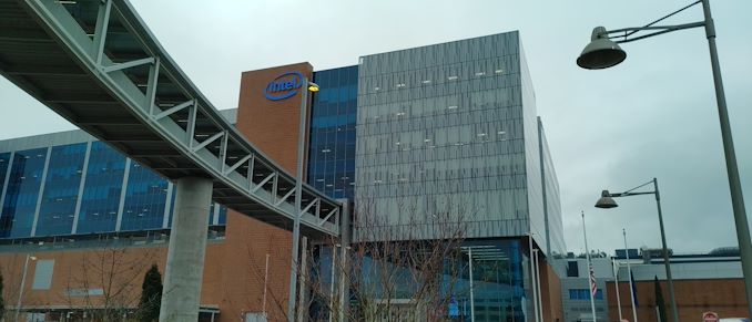
On a recent trip to the US, I decided to spend some time criss-crossing the nation for a couple of industry events and spend some of the time visiting friends and peers. One of those stops was at Intel’s D1X Fab in Hillsboro, Oregon, one of the company’s leading edge facilities used for both production and development. It’s very rare to get time in a fab as a member of the press – in the ten years covering the industry, I’m lucky to say this was my second, which is usually two more than most. As you can imagine, everything had to be pre-planned and pre-approved, but Intel managed to fit me into their schedule.

Samsung Foundry: New $17 Billion Fab in the USA by Late 2023
Samsung Foundry has filed documents with authorities in Arizona, New York, and Texas seeking to build a leading-edge semiconductor manufacturing facility in the USA. The potential fab near Austin...
36 by Anton Shilov on 2/10/2021
Intel’s Manufacturing Roadmap from 2019 to 2029: Back Porting, 7nm, 5nm, 3nm, 2nm, and 1.4 nm
One of the interesting disclosures here at the IEEE International Electron Devices Meeting (IEDM) has been around new and upcoming process node technologies. Almost every session so far this...
138 by Dr. Ian Cutress on 12/11/2019
Hot Chips 31 Keynote Day 2: Dr. Phillip Wong, VP Research at TSMC (1:45pm PT)
The keynote for the second day is from TSMC, with Dr. Phillip Wong taking the stage to talk about the latest developments in TSMC's research and portfolio. The talk...
12 by Dr. Ian Cutress on 8/20/2019
Intel to Fab Altera FPGAs with ARM IP
In a story posted today on EETimes, Altera announced at the ARM Developers Conference that they have entered into a partnership with Intel to have their next generation 64-bit...
44 by Jarred Walton on 10/30/2013


