Analyzing Falkor’s Microarchitecture: A Deep Dive into Qualcomm’s Centriq 2400 for Windows Server and Linux
by Ian Cutress on August 20, 2017 11:00 AM EST- Posted in
- CPUs
- Qualcomm
- Enterprise
- SoCs
- Enterprise CPUs
- ARMv8
- Centriq
- Centriq 2400
Enterprise Features: Security
With security being a strong focal point in data center tasks, all of the major players that want to provide processors for cloud deployments have been getting their hands dirty and talking security. The ability to provide security keys for hypervisors, VMs, and everything else that can be sandboxed from other users is paramount. To this extent, the Centriq 2400 is supporting two levels of security: EL3 and EL2. This means TrustZone at a system level (EL3) as well as a hypervisor level (EL2), although Qualcomm has not gone into detail if this extends through to having some VMs secure and others not within the same hypervisor environment. Where some of Qualcomm’s competitors are using ARM’s TrustZone implementation – which is an ARM Cortex-A5 for the management – Qualcomm has stated that their solution is not ARM based but a custom design that is TrustZone compliant. We confirmed that this wasn’t another re-use of an ARM architecture license.
Also for security, Qualcomm has added instructions geared towards cryptography acceleration, supporting AES, SHA1, and SHA2-256.
Enterprise Features: Secure Boot
Implementing a Root of Trust has also being making the rounds in recent years. With nefarious code potentially rewriting firmware, or zero-day flaws in technology being exploited by friend and foe, being able to verify the underlying system is as intended and only as intended becomes paramount. Qualcomm’s Centriq 2400 will use Secure Boot functionality.
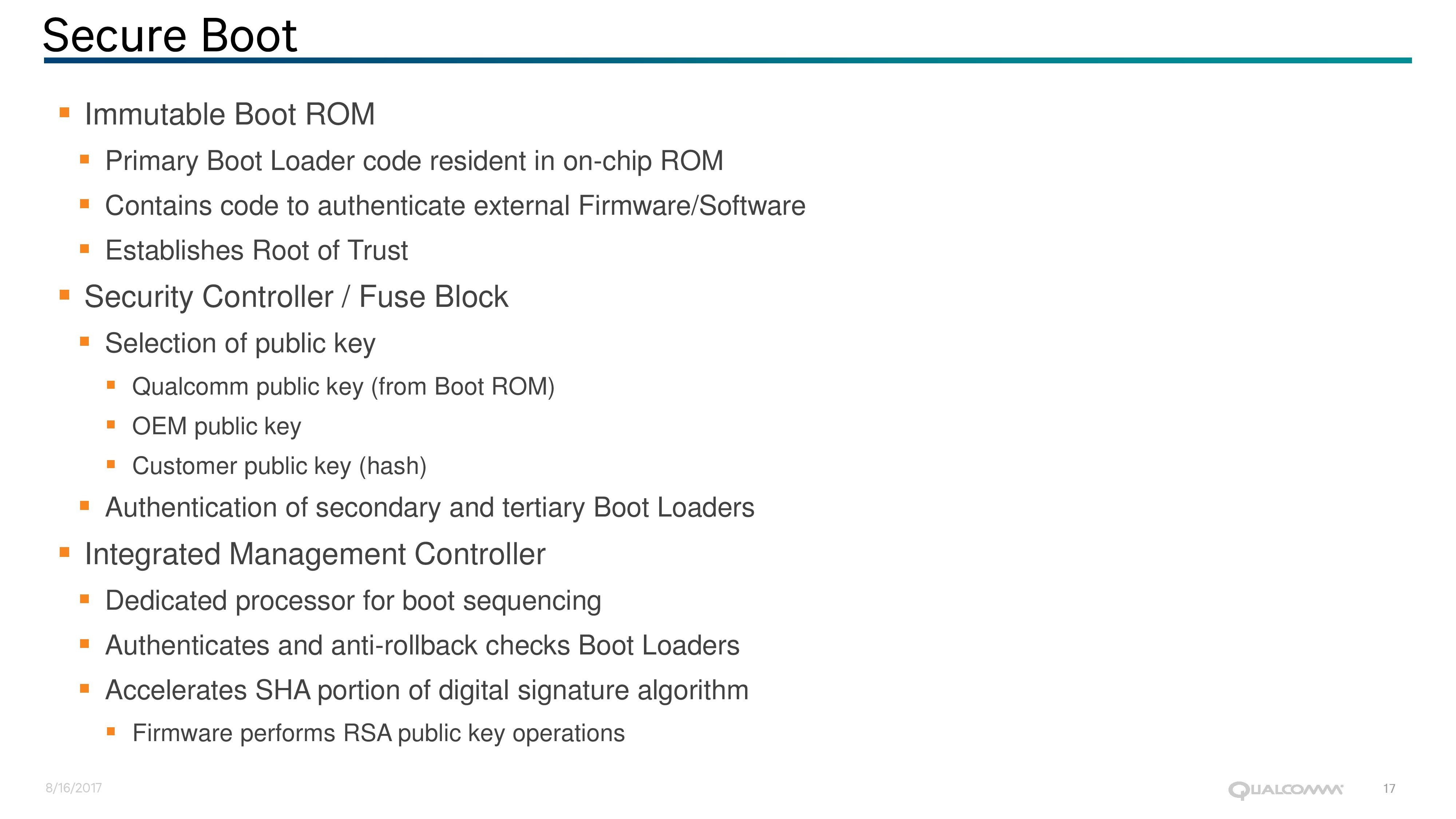
This is accomplished by providing an Immutable Boot ROM via an integrated management controller, with burned in code and cryptographic keys to authenticate firmware and software before any other firmware is loaded. Qualcomm states that this guarantees knowledge of ownership at the base level, as it allows customers to store (at purchase) public keys from Qualcomm, the OEM or the customer to authenticate secondary and tertiary bootloaders with an anti-rollback check. The management controller also supports accelerated cryptography on SHA for digital signatures and RSA public key operations.
Enterprise Features: QoS
Also on the cards is L3 quality of service. In shared resource environments, mission critical applications can be disturbed by ‘noisy neighbors’. With multiple virtual machines vying for the same resources on a single machine, issues such as shared cache contention have flared up in recent quarters for data center use. If one VM is relying on consistent performance from memory accesses from cache but another program is thrashing it and causing inconsistent performance, the user experience can noticeably be disturbed.
There are multiple ways to tackle this, such as increasing the amount of private cache per core/VM, or by providing L3 cache Quality of Service (QoS) features. Intel has done both in recent years, such as increasing the amount of L2 private cache on the Skylake-SP Xeons from 256KB to 1MB, as well as offering L3 QoS since Broadwell-EP. AMD uses 512KB of L2 private cache, and also has QoS in play. Qualcomm isn’t disclosing the amount of L2 or L3 cache in today’s announcement, but were happy to discuss their QoS strategy.
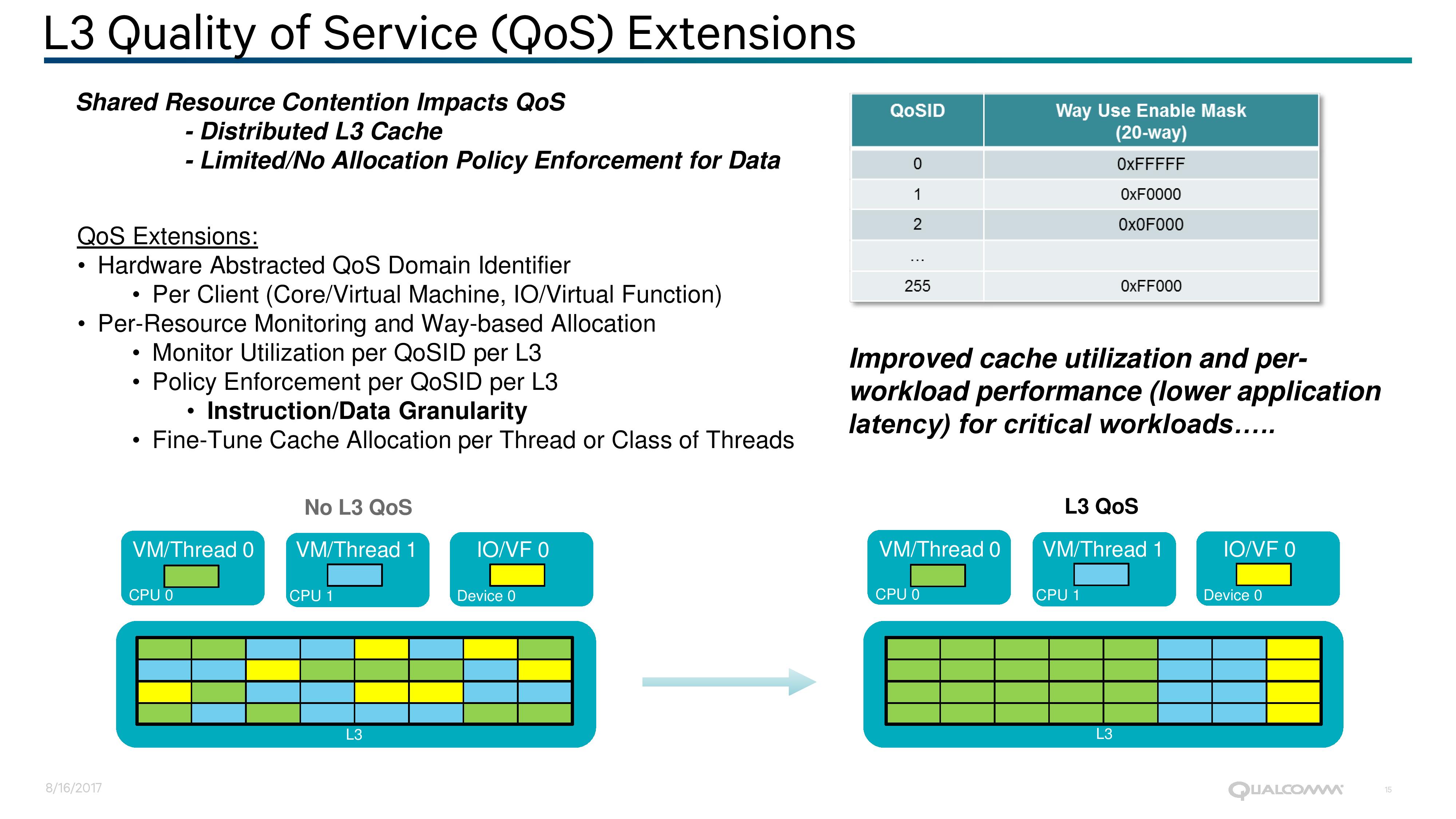
Qualcomm has stated (despite some odd diagrams perhaps suggesting otherwise) that the L3 cache in the Centriq family is a distributed cache, which likely means that each core (or Duplex, more on that later) has a certain amount of associated L3 cache and L3 cache tags with it. By using a hardware abstracted QoS identification method per client, the SoC can monitor resources and enforce L3 QoS policies per domain ID and per L3 segment, down to the instruction and data level granularity. This is done using Way-based allocation, and policies can be adjusted or fine-tuned on the fly per thread or class of threads. Qualcomm’s implementation can support up to 256 defined environments, one of which can be designated or the SoC IO.
Enterprise Features: Memory Bandwidth Compression
One of Qualcomm’s angles in the data center space is going to be that many data center workloads are memory bandwidth constrained. ‘Feeding the Beast’ is the limit for the markets they want to enter, so by enabling transparent memory compression out to DRAM, Qualcomm is attempting to address the issue. This feature will be transparent to any software, with the effect seen mostly in compressible data streams and memory streaming benchmarks.
By using a proprietary algorithm, Qualcomm’s inline compression will attempt to reduce a 128-byte cache line to 64-bytes with ECC as it moves into main memory. When recalling the data back into the core or for committing to storage, decompression adds an additional 2-4 cycles (1-2% on 250-cycle latency) but aims to bring more data in per request than uncompressed data. There could be a slight added benefit of lower power consumption as well, as less data is transferred. We’ve seen these techniques in the GPU space for a number of years.

From the software perspective, the effect will vary considerably from test to test depending on the workload. The Centiq 2400 series comes with six DDR4 memory channels, supporting two DIMMs per channel and up to DDR4-2667, so there’s going to be a lot of bandwidth to begin with – but sometimes that just isn’t enough.


41 Comments
View All Comments
SarahKerrigan - Sunday, August 20, 2017 - link
I seriously doubt SVE is present. As far as I know, Fujitsu is still lined up to be the first SVE user, and it's not like ultra-wide vectors are a massive boost to conventional enterprise servers.Kevin G - Sunday, August 20, 2017 - link
Using SVE requires ARM v8.2A support which this does not appear to have. The ARM v8.2A spec only was announced in January 2016, which isn't enough time to get it implemented into anything that'd be shipping now. Qualcomm could have been working behind the scenes but that would have given them perhaps another year with a spec that could change before formal publishing (i.e. may require some last minute changes right past the design would be tapping out). For a server part, that path would be unwise.SVE was announced a year ago and is far more complex than the v8.2A released due to how it handles execution width. A SVE design right now is a virtual impossibility.
Hurr Durr - Sunday, August 20, 2017 - link
I`d rather read something on x86 thing on ARM that MS and Qualcomm have than this. Much more potential for the real world.Kevin G - Sunday, August 20, 2017 - link
Can we get an editor in here?"For SoC design followers, one might look at this design and think they see similarities with designs such as AMD’s original Bulldozer design from 2011. ... Actually, after writing that last sentence, it is basically a Xeon Phi dual core module."
While perfectly readable, that last paragraph could use a bit of a rewrite due to the last sentence nullifying it. My quick stab at a rewrite:
For SoC followers, the Qualcomm pairs two modules per fabric stop similar to what Intel has implemented in their most recent Xeon Phi chips. Unlike the new grid topology in the Xeon Phi, Qualcomm is using a ring bus akin to what Intel uses on its Xeon E5 and E7 chips. Those thinking that a dual core module would follow AMD's Bulldozer philosophy will be disappointed to learn that no execution resources are shared between the cores, just the L2 cache, power management and bus interface.
The same comparisons and ideas are made but they flow to the reader a bit more logically to me.
FunBunny2 - Sunday, August 20, 2017 - link
-- Unlike the new grid topology in the Xeon Phi, Qualcomm is using a ring bus akin to what Intel uses on its Xeon E5 and E7 chips.I've long wondered how hardware engineers:
1) discover such alternatives
2) decide which one to choose
Is this fundamental math and physics laws, or trial and error? anyone know a readable (for the non-physics major, that is) source?
Kevin G - Monday, August 21, 2017 - link
Topology has been a well studied concept. At a high level, this mimics general networking design closely. The choice of on-die topology is generally at the mercy of engineering trade offs that are unique in this context.The ring bus you get an easy means of scaling the number of units but the trade of is an increase in latency around the ring bus as the numbers go up. Diminishing returns are hit as the numbers increases. With a ring though, individual units on the ring can be radically different sizes on a die as long the links between stops can be roughly the same for timing purposes. A ring bus also permits a relatively predictable latency to reach stops further away, something noteworthy for implementing coherency protocols. Another trade off with the ring design is that it'll always consume power. Nodes that are not in use still need to have the ring stop going to permit data passage through it.
Qualcomm side steps the ring issue a little bit by including two cores per ring stop, thus putting the minimum number of stops at 24. Just like Intel, I suspect on-die IO like PCIe, memory controllers etc. will have their own ring stops. It is not clear if this all on one massive ring bus or like the last generation of E5/E7 high core count chips, several rings are used with discrete bridges between them. Intel never went beyond 16 ring stops in a design.
A grid topology requires far greater engineering resources to implement correctly. Physical size has to be the same for those nodes in the middle of the grid but there is a bit of wiggle room along the perimeter to expand in one of the two dimensions (handy for things like PCIe, memory controllers that have a fixed need per socket). Cache coherency has to account for variable latency between nodes on the grid: there are several paths to between source and destination. The main benefit of a grid though is that scaling is vastly improved as core count increases. Another benefit is that not all the links in between cores needs to be active to move data. This saves power. Due to the ability to route around congested links, the individual links between grid nodes do not necessarily have to be as wide as those on a ring, saving a bit of energy there while maintaining similar aggregate bandwidth. For servers, multi-pathing of data (ie sending it twice) is also possible for increased RAS if an error in transmit is encountered along a particular path. Intel hasn't indicated that they're doing multipathing but could be a feature they add down the road. In the future if chips stacking emerges outside of research labs as feasible, the grid topology can also expand into the 3rd dimension.
The recent Xeon Phi isn't Intel's first attempt at a grid topology. The first publiclly shown off design was there Terascale research chip a decade ago. ( http://www.eetimes.com/document.asp?doc_id=1303295 ) Inter core topology was a major driver of that research effort and the recent Xeon Phi and Xeon series are the result of those efforts. Intel isn't event the first to implement a grid topology. The Compaq/DEC Alpha EV7 did so between sockets and permitted up to 64 sockets in an 8 x 8 grid from the early 2000's. IBM used a grid-like design for their BlueGene super computer designs to move data, though that wasn't cache coherent. There could be earlier instances as those are a few that I know off hand.
FunBunny2 - Monday, August 21, 2017 - link
thanks. much clearer.Ryan Smith - Sunday, August 20, 2017 - link
Thanks!Lord-Bryan - Sunday, August 20, 2017 - link
"So we have to admit that we were surprised by Qualcomm releasing so much information about the pipeline. When we’ve ever asked the mobile CPU team about Krait and Kryo, we usually hit a brick wall, left with a PR answer of a ‘custom core design’ or the guide of ‘protecting our design"Well am not surprised, releasing architectural details of server cpus, has always been an industry norm. It is something they just have to do if they want to be relevant, you can't just sell black boxes worth thousands of dollars to just anyone.
Lord-Bryan - Sunday, August 20, 2017 - link
Plus developers will have to know how the processor works in other to optimize applications for it, Qualcomm is playing with the big boys now, no room for unnecessary pride.