Arm Announces Neoverse N1 & E1 Platforms & CPUs: Enabling A Huge Jump In Infrastructure Performance
by Andrei Frumusanu on February 20, 2019 9:00 AM ESTE1 Implementation & Performance Targets
The Neoverse E1 CPU being a small CPU core aimed at cost-effective and dense implementation naturally needs to be quite small, as well as power efficient.
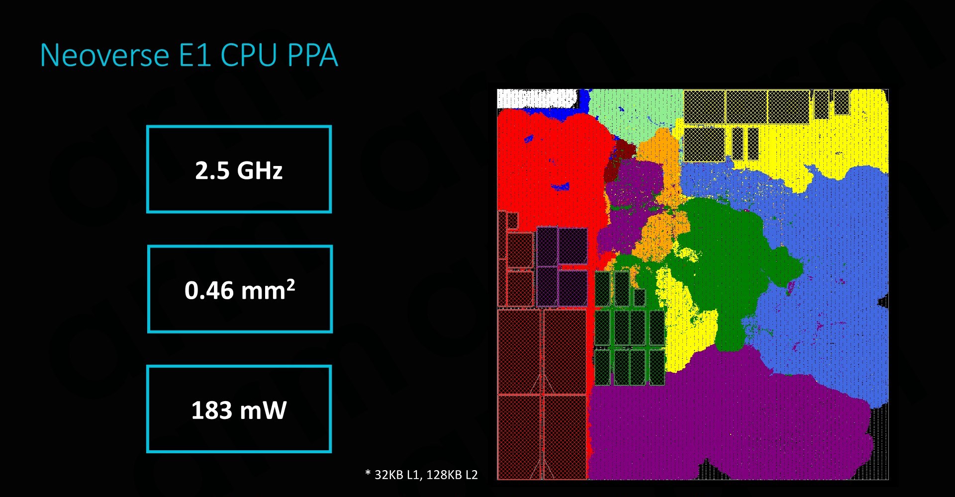
Implemented on a 7nm process, Arm physical design team is able to get an E1 CPU core with 32KB L1 and 128KB L2 cache down to 0.46mm² - all while reaching a high clock of 2.5GHz and a power consumption of 183mW. The higher clock was a surprise as it is quite notably higher than what we’ve seen vendors achieve on the A55 – although we are talking about different implementation targets.
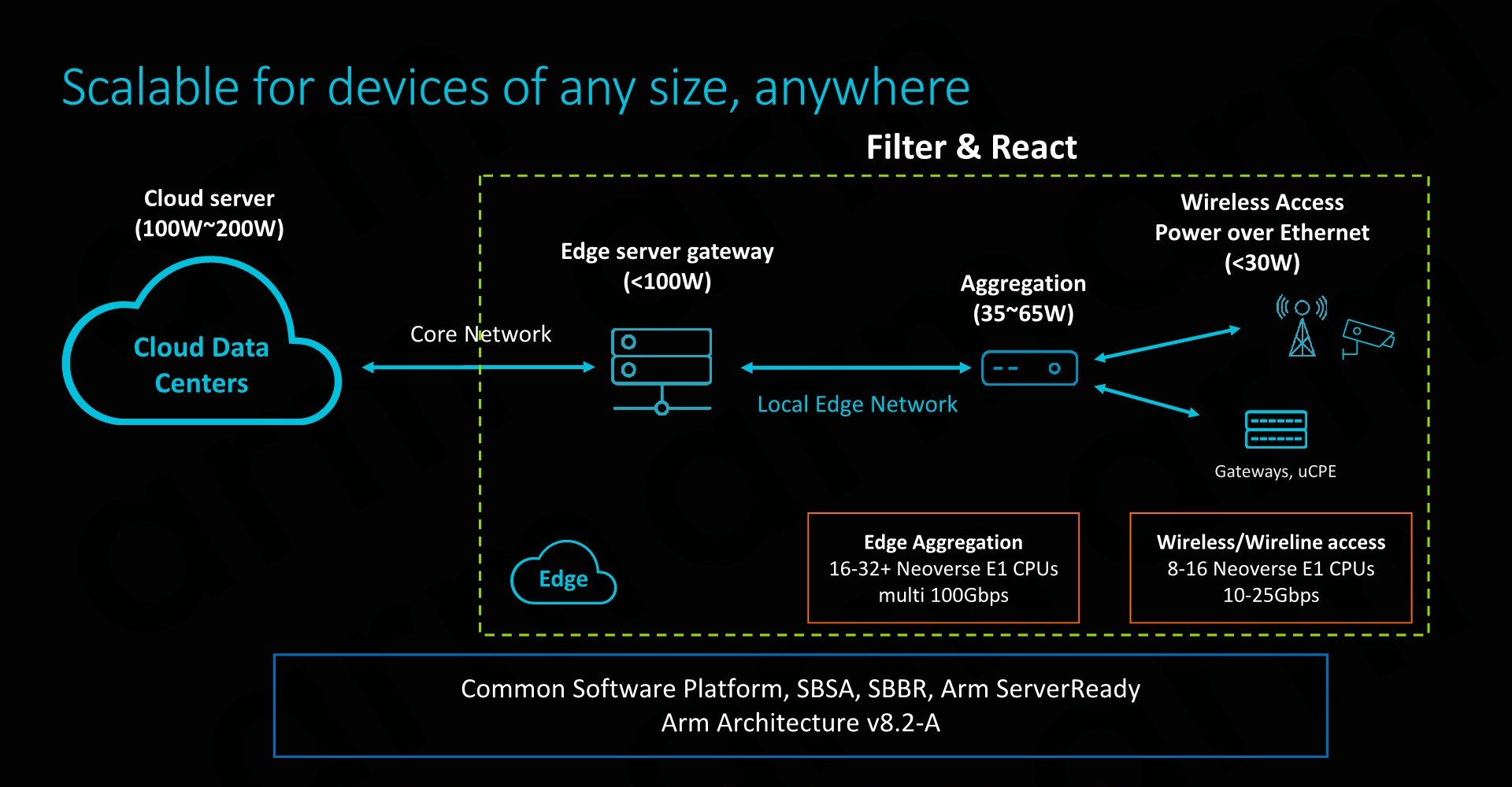
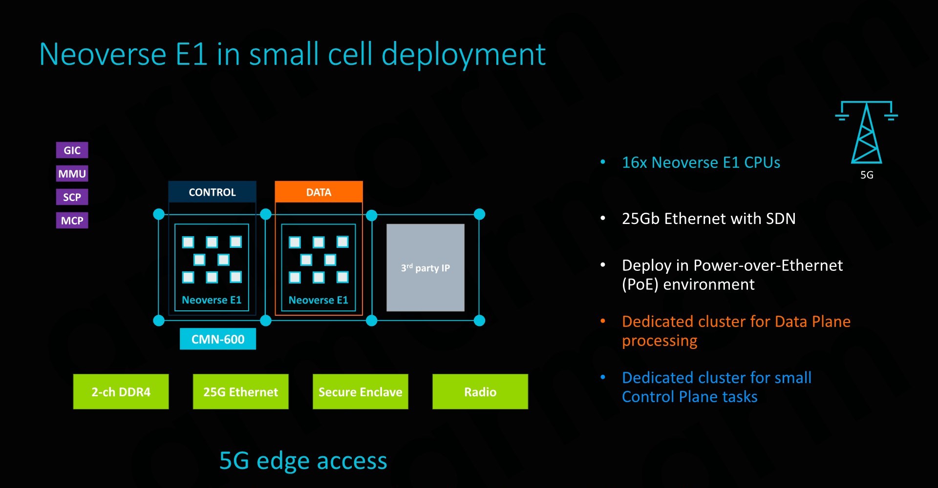
Arm envisions the most popular implementations of the E1 to be found in lower power edge applications. At the lower end, ranging from 8-16 cores would be a good for wireless access points and gateways, delivering data throughputs in the 10-25Gbps rang. A tier up we would see 16-32 core designs in use-cases such as edge data aggregation deployments, achieving data rates in the 100’s of Gbps.
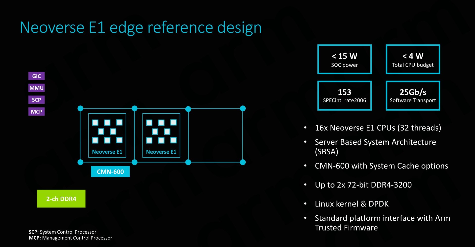
The Neoverse E1 reference design that Arm offers and sees as being the most popular “sweet-spot” is based on a 16 core design. Here we have to clusters of 8 cores in a small CMN-600 2x4 mesh network, allowing for system cache options as well as integration of possible additional third-part IP. The envisioned memory system would be a 2-ch DDR4 configuration.
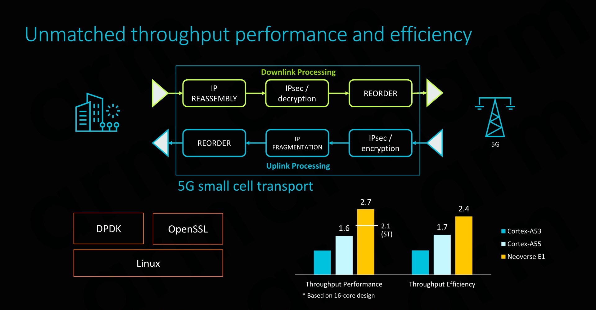
Such as SoC would have a power consumption of less than 15W, of which less than 4W would actually be used by the CPU cores. SPECint2006 rate scores would come in at 153 – which given the actual size and power consumption of the platform is quite impressive. The system would also be capable of 25Gb/s network throughput, enabled solely by a software transport layer (Meaning no hardware acceleration).
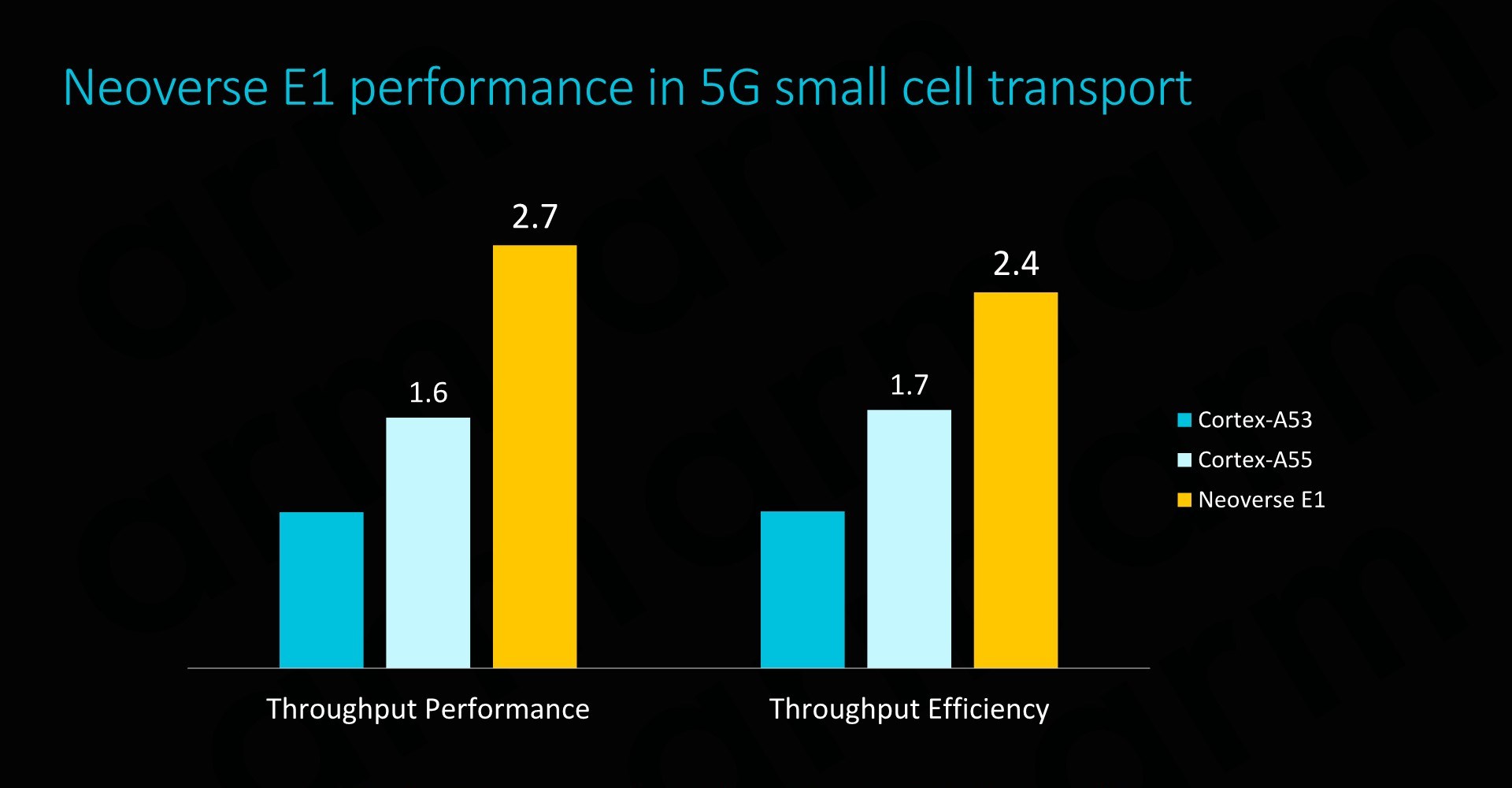
On a per-core comparison to the Cortex A53 and A55, the new E1 CPU would again offer significant throughput performance benefits, but also very importantly it would represent an efficiency boost compared to its predecessors (ISO process comparison).


101 Comments
View All Comments
Santoval - Thursday, February 21, 2019 - link
"Both Intel and AMD have been making chips that take the CISC instructions and run them through an instruction decoder that then hands RISC instructions to the actual cpu."The instruction decoder is also part of an "actual CPU". Beside the decoder the front-end also has instruction fetch, a branch predictor, predecode (potentially), μOP & L1 instruction cache, instruction queues, a TLB, allocation queues etc etc All these units are most certainly parts of the "actual CPU".
I believe you rather meant "hands RISC-like instructions to the *back-end* of the CPU".
FunBunny2 - Thursday, February 21, 2019 - link
"The speed advantages on paper between RISC and CISC are in theory a wash. "not to keep beating the dead horse 360, dated as it is, but with the hardware of the time (and IBM was the top of the heap, then) the 360/30 ran the instruction set in micro-code. allegedly the first computer to even have microcode. ran like drek compared to the all-hardware versions of the machine. the '30 real cpu was long reputed to be some DEC machine.
"cpu design quite a bit without being so closely tied to backwards compatibility."
lots of folks say that, but makes no sense to me. compilers target the instruction set, which only changes when Intel publishes 'extensions'. whether those instructions are executed in pure ISA hardware, or a rat running in a spinning wheel (RISC), makes no difference to the compiler writer.
the profiling explanation for microcode over pure ISA hardware makes the most sense.
Wilco1 - Wednesday, February 20, 2019 - link
The only misinformation is from you. RTL simulation is widely used in the industry and is quite accurate.Studies have shown CISC instructions don't do more than RISC instructions - partly because compilers avoid CISC instructions, partly because CISC instructions are slow. That's why RISC works. But I wouldn't expect you to understand this.
FunBunny2 - Thursday, February 21, 2019 - link
"Studies have shown CISC instructions don't do more than RISC instructions "at least in the z world (and predecessors), there were/are some (I don't remember the count) of 'COBOL assist' instructions which were/are quite complex and were introduced to reduce the amount of times the COBOL coders had to 'drop down to assembler'. whether that's still true, I can't say.
DigitalVideoProcessor - Thursday, February 21, 2019 - link
CISC vs. RISC is a debate about instruction decode philosophy and it has almost zero bearing on the performance of a system. CISC machines reduce everything to RISC like operations. Saying one does more than another in a given clock is misinformation.melgross - Thursday, February 21, 2019 - link
Those wars are long over. No modern chip is either pure CISC or RISC. Those are long gone.Calin - Thursday, February 21, 2019 - link
SPECint, SPECfp, ... are "work done tasks" - what your're referring to was "MIPS" (or millions of instructions per second). This performance metric has lost its charm since internally x86 processors no longer use x86 instructions but large bundles of microoperations that are done in parallel and can be interleaved (so two instructions that follow each other are broken into micro operations which are reordered, and might be finalized in a different order).Kevin G - Thursday, February 21, 2019 - link
The thing is that real distinction of CISC vs. RISC is lost in their similar implementations: pipelined OoO parallel execution engines. While CISC encoding may* permit more operations to be contained within a single instruction but at the cost of having to decode that instruction into an optimal arrangement given the hardware. The price paid is in power consumption and complexity which may impact factors like maximum clock speed. In the era of many core and power limitations, these attributes are the foundation for RISC to have an edge over legacy CISC designs. Not to say that RISC architectures can't leverage instruction decoding either: expanding out the fields for registers to account for the larger rename register space is a simple procedure.Once chips begin parallel execution, the CISC advantage of doing more per instruction really starts to fall apart. The raw amount of work being done per cycle approaches the common limit of just how much parallelism can be extracted by an inherently serial stream of instructions. Arguably CISC designs can hit this sooner in terms of raw instruction count as the instruction stream is _effectively_ compressed compared to RISC.
*The concept of fused-multiply add instructions was an early staple of RISC architectures. Technically it goes against the purest ideal but traditional RISC designs permitted the number of operands in their instruction formatting to pull this off so they took advantage of an easy performance boost. x86 didn't gain this capability until AVX2 a few years ago.
peevee - Tuesday, February 26, 2019 - link
"I think you are forgetting the very nature of RISC (Arm) vs CISC (x86) architectures"This distinction does not exist in practice for decades.
wumpus - Wednesday, February 20, 2019 - link
It also shows a result showing Zen roughly half the performance of Intel, something that implies a fairly contrived situation. FX8350 might have had half (or worse) than Intel, but Zen is another story.I'm guessing that this involves AVX256 (or higher) specifically optimized for Intel (note that going to AVX512 is only a modest increase since the clockrate is brutally lowered to compensate for the increased power load. Also note that Zen2 (EPYC2 and Ryzen3000) will include native AVX256 execution paths).