Arm Announces Neoverse N1 & E1 Platforms & CPUs: Enabling A Huge Jump In Infrastructure Performance
by Andrei Frumusanu on February 20, 2019 9:00 AM ESTE1 Implementation & Performance Targets
The Neoverse E1 CPU being a small CPU core aimed at cost-effective and dense implementation naturally needs to be quite small, as well as power efficient.
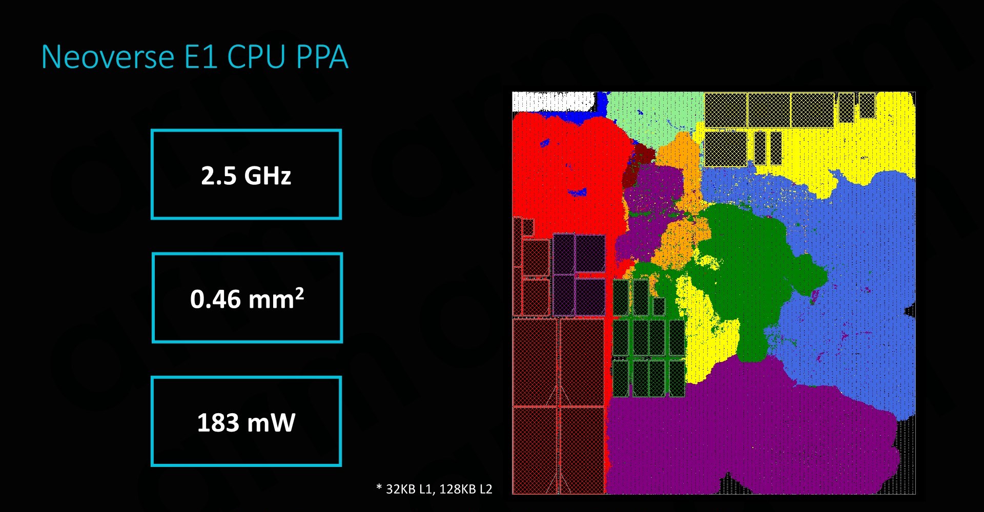
Implemented on a 7nm process, Arm physical design team is able to get an E1 CPU core with 32KB L1 and 128KB L2 cache down to 0.46mm² - all while reaching a high clock of 2.5GHz and a power consumption of 183mW. The higher clock was a surprise as it is quite notably higher than what we’ve seen vendors achieve on the A55 – although we are talking about different implementation targets.
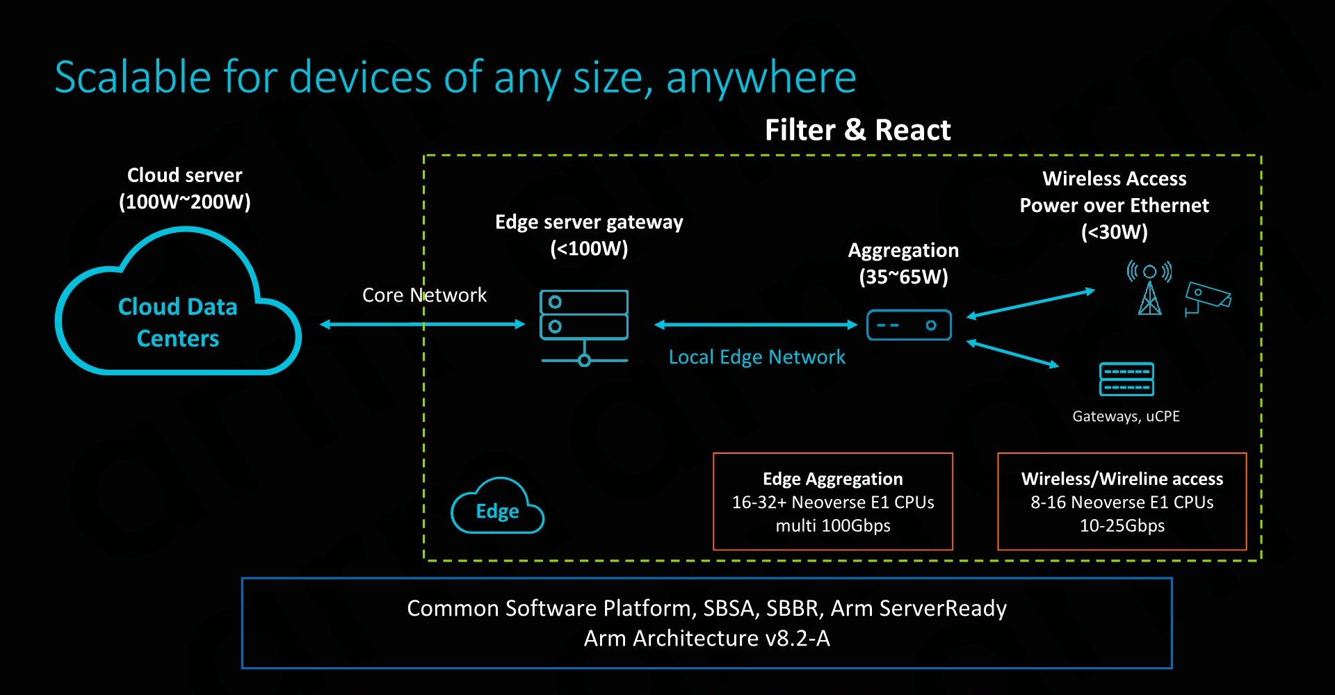
Arm envisions the most popular implementations of the E1 to be found in lower power edge applications. At the lower end, ranging from 8-16 cores would be a good for wireless access points and gateways, delivering data throughputs in the 10-25Gbps rang. A tier up we would see 16-32 core designs in use-cases such as edge data aggregation deployments, achieving data rates in the 100’s of Gbps.
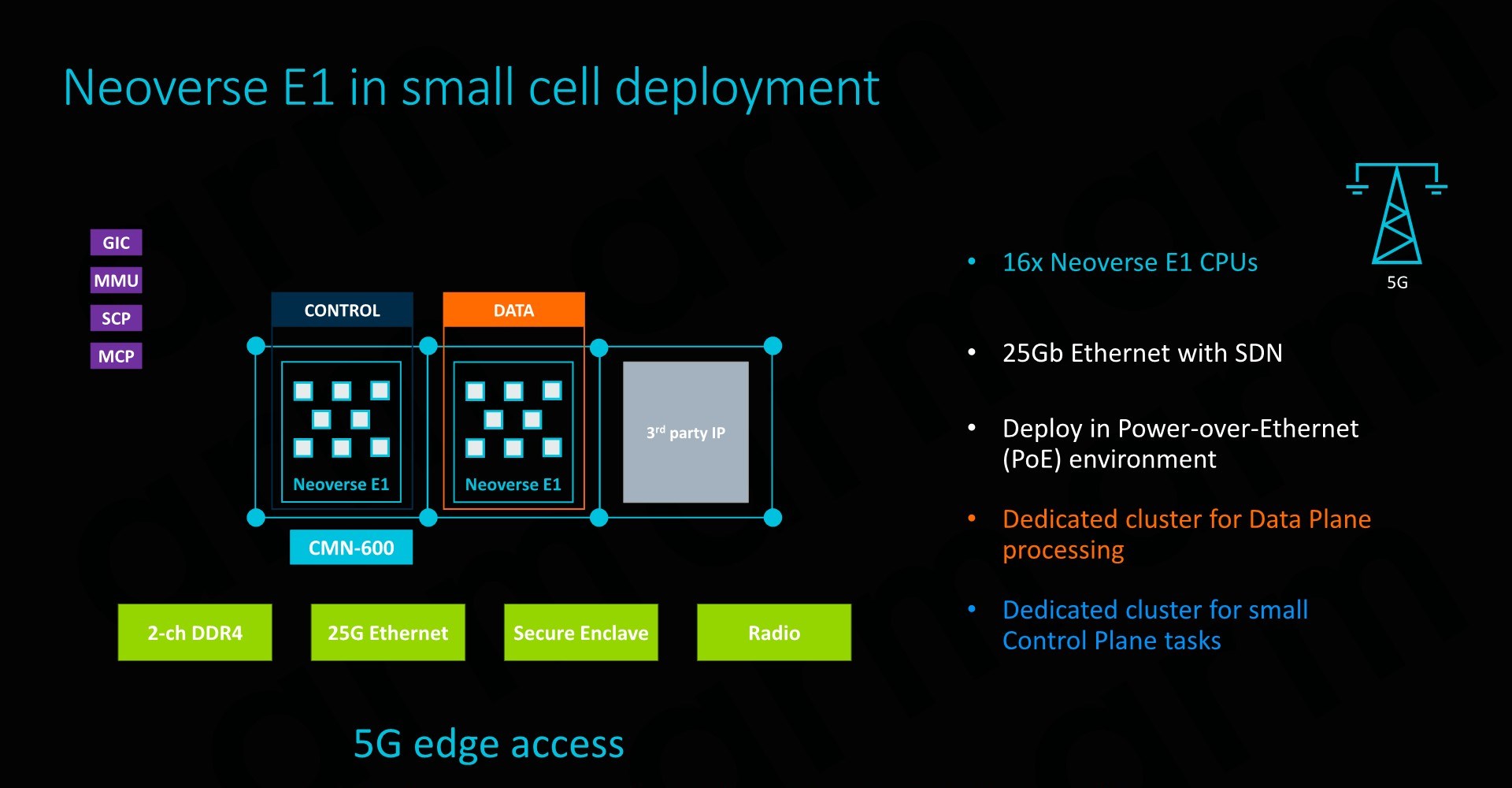
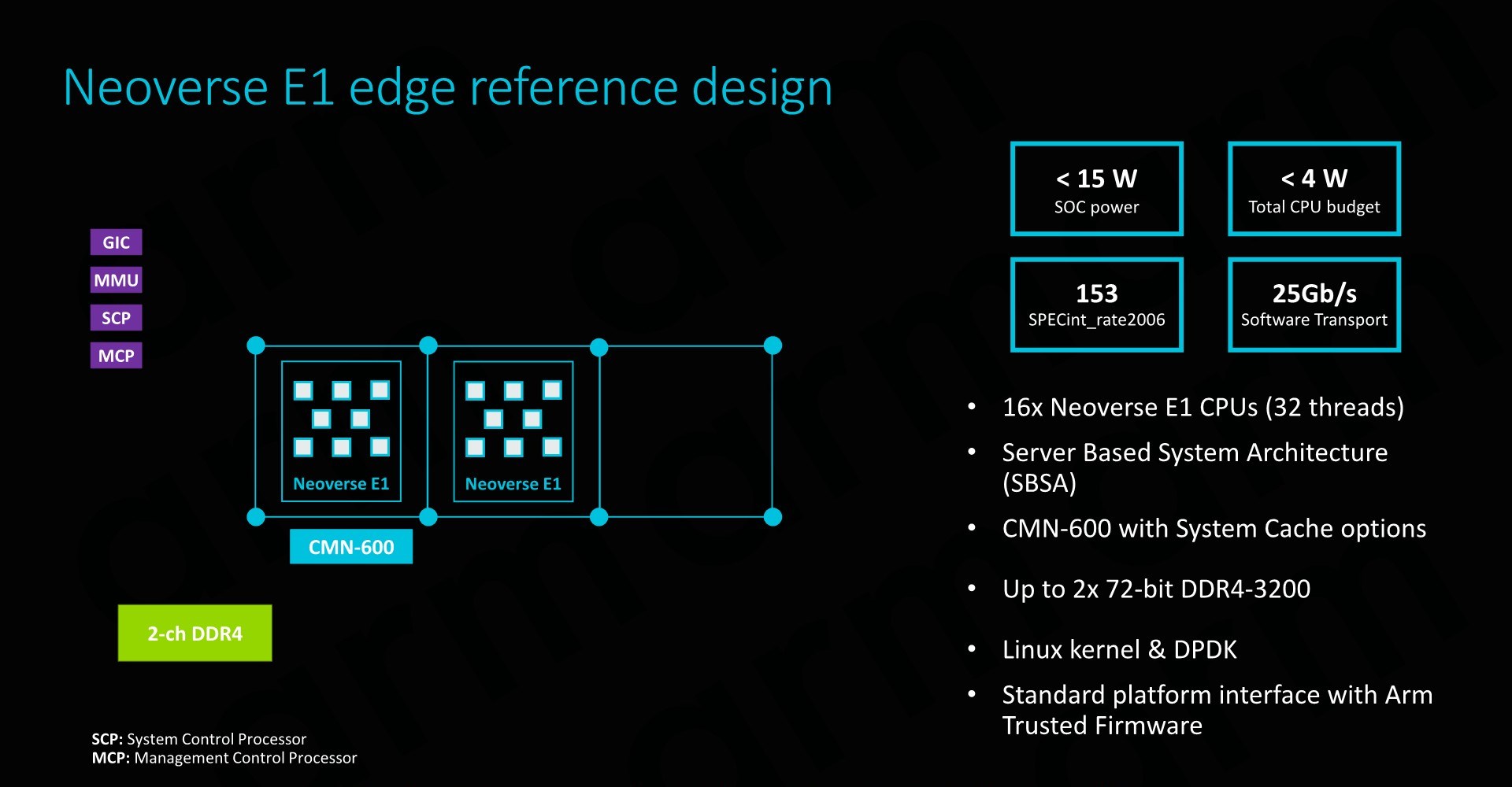
The Neoverse E1 reference design that Arm offers and sees as being the most popular “sweet-spot” is based on a 16 core design. Here we have to clusters of 8 cores in a small CMN-600 2x4 mesh network, allowing for system cache options as well as integration of possible additional third-part IP. The envisioned memory system would be a 2-ch DDR4 configuration.
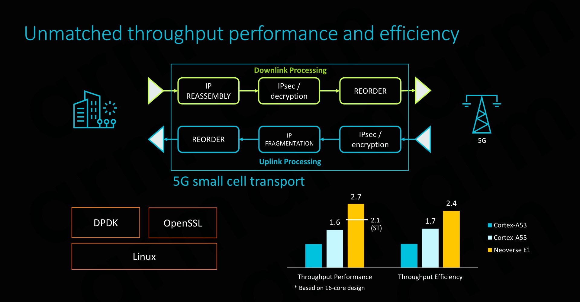
Such as SoC would have a power consumption of less than 15W, of which less than 4W would actually be used by the CPU cores. SPECint2006 rate scores would come in at 153 – which given the actual size and power consumption of the platform is quite impressive. The system would also be capable of 25Gb/s network throughput, enabled solely by a software transport layer (Meaning no hardware acceleration).
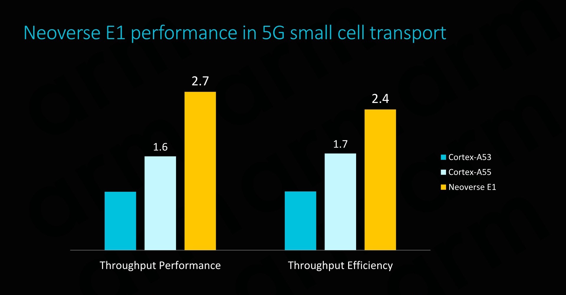
On a per-core comparison to the Cortex A53 and A55, the new E1 CPU would again offer significant throughput performance benefits, but also very importantly it would represent an efficiency boost compared to its predecessors (ISO process comparison).


101 Comments
View All Comments
Andrei Frumusanu - Wednesday, February 20, 2019 - link
> It also shows a result showing Zen roughly half the performance of IntelThe W-3175X was at 4.5GHz with the whole 38MB of L3 for the one thread, while the 7601 ran at a peak of 3.2GHz.
Meteor2 - Wednesday, February 20, 2019 - link
I wish you’d normalised for frequency!Andrei Frumusanu - Wednesday, February 20, 2019 - link
That's not the point of the article.ZolaIII - Wednesday, February 20, 2019 - link
Next time read twice before posting. AVX on integer benchmark really?Wilco1 - Wednesday, February 20, 2019 - link
Of course. Never heard of how SIMD hugely affects libquantum for example?Andrei Frumusanu - Wednesday, February 20, 2019 - link
AVX works on integer ...ZolaIII - Wednesday, February 20, 2019 - link
The era of general purpose core's being used for HPC is long time gone. While general purpose core's are hire to stay they will do that with modest number of core's per system, the real push is towards special purpose and multi purpose accelerators. FPGA's being put in the first row because their reprogrammable nature. The ARM actually have an edge over the CISC (X86) because it's simply more efficient which having stellar integer performance for the size of the core. If you look at the development bord it's very clear ARM is pushing into right direction.Meteor2 - Wednesday, February 20, 2019 - link
Kind of. But bottom line is the 20-odd codes used predominantly in the world still run best on general purpose CPUs. Bending software to work on specialised architectures is really hard.ZolaIII - Thursday, February 21, 2019 - link
On the FPGA you bend hardware. That's the whole idea.wumpus - Thursday, February 21, 2019 - link
HPC traditionally meant double precision FLOPS. AI work or similar might want FPGAs until GPUs are sufficiently ready for such things (then FPGA can't keep up).FPGAs are painfully slow at what they do, but can take an entirely new architecture on the fly. We saw that with cryptomining as things went CPU->GPU->FPGA->ASIC. And if you need a lot of multiply-accumulate (like most AI), don't expect anything between GPU and ASIC.