Arm Announces Neoverse N1 & E1 Platforms & CPUs: Enabling A Huge Jump In Infrastructure Performance
by Andrei Frumusanu on February 20, 2019 9:00 AM ESTE1 Implementation & Performance Targets
The Neoverse E1 CPU being a small CPU core aimed at cost-effective and dense implementation naturally needs to be quite small, as well as power efficient.
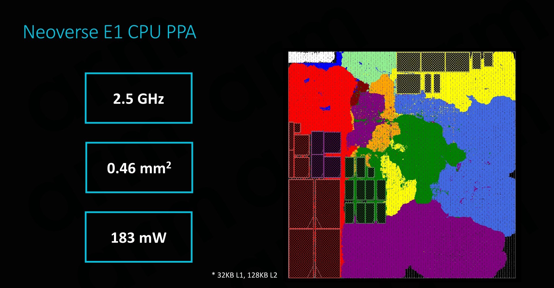
Implemented on a 7nm process, Arm physical design team is able to get an E1 CPU core with 32KB L1 and 128KB L2 cache down to 0.46mm² - all while reaching a high clock of 2.5GHz and a power consumption of 183mW. The higher clock was a surprise as it is quite notably higher than what we’ve seen vendors achieve on the A55 – although we are talking about different implementation targets.
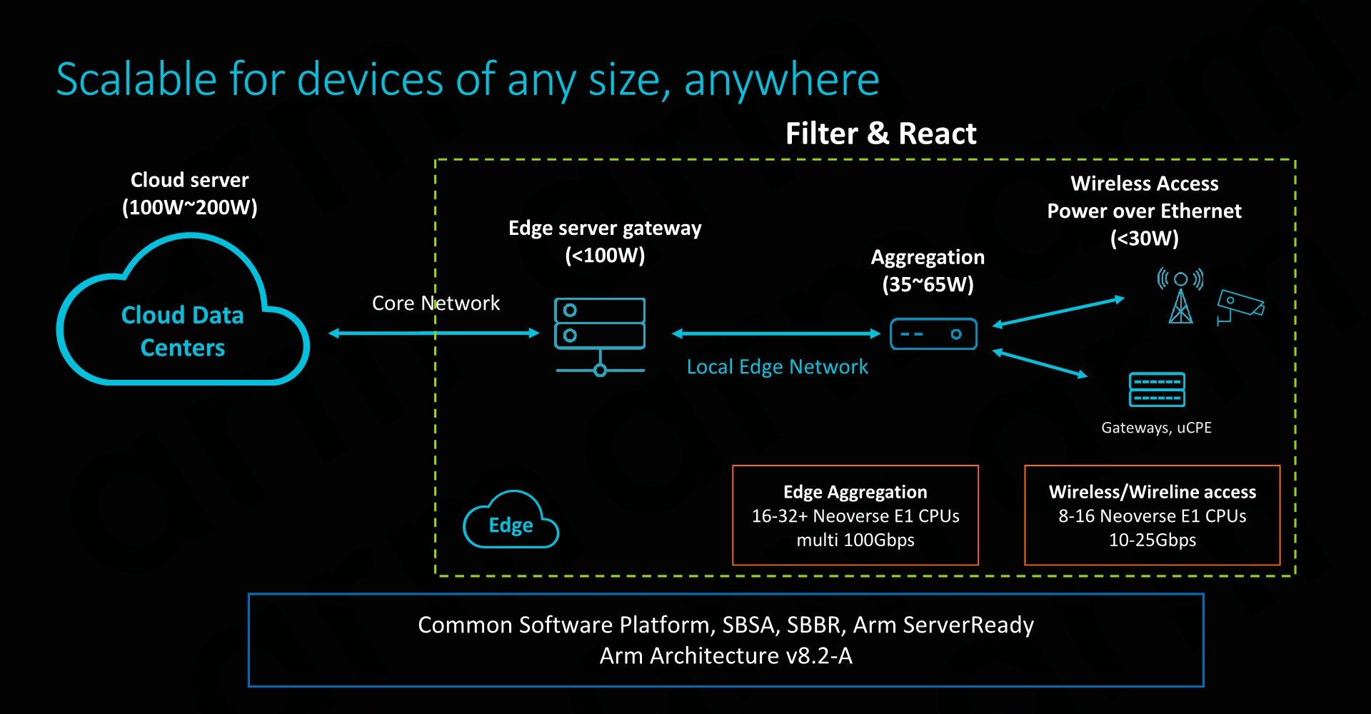
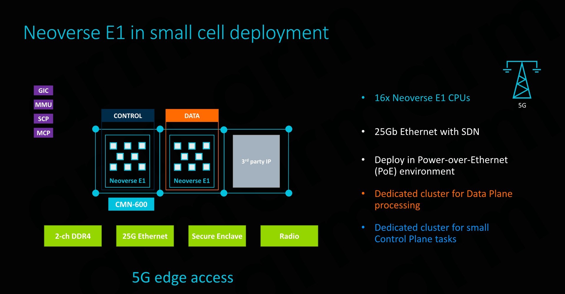
Arm envisions the most popular implementations of the E1 to be found in lower power edge applications. At the lower end, ranging from 8-16 cores would be a good for wireless access points and gateways, delivering data throughputs in the 10-25Gbps rang. A tier up we would see 16-32 core designs in use-cases such as edge data aggregation deployments, achieving data rates in the 100’s of Gbps.
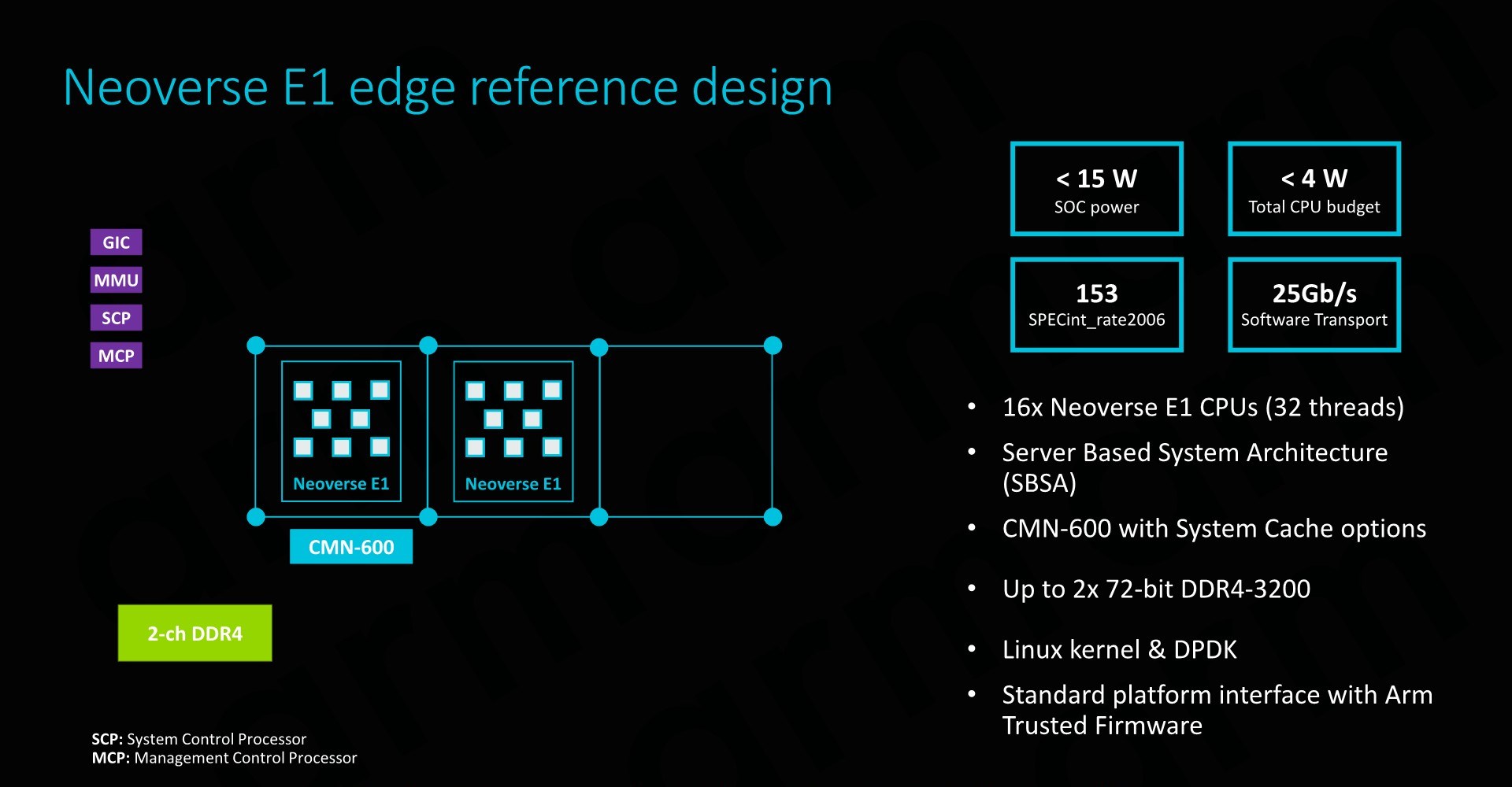
The Neoverse E1 reference design that Arm offers and sees as being the most popular “sweet-spot” is based on a 16 core design. Here we have to clusters of 8 cores in a small CMN-600 2x4 mesh network, allowing for system cache options as well as integration of possible additional third-part IP. The envisioned memory system would be a 2-ch DDR4 configuration.
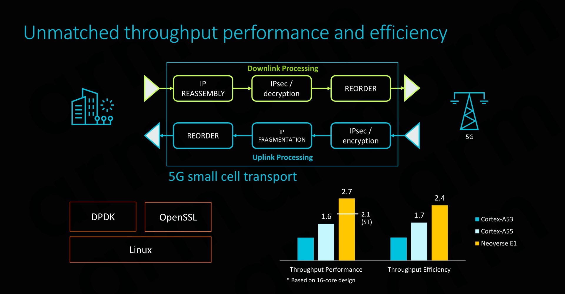
Such as SoC would have a power consumption of less than 15W, of which less than 4W would actually be used by the CPU cores. SPECint2006 rate scores would come in at 153 – which given the actual size and power consumption of the platform is quite impressive. The system would also be capable of 25Gb/s network throughput, enabled solely by a software transport layer (Meaning no hardware acceleration).
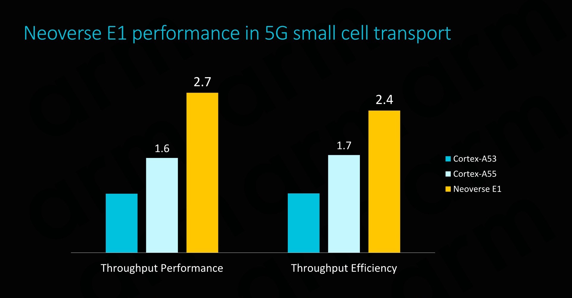
On a per-core comparison to the Cortex A53 and A55, the new E1 CPU would again offer significant throughput performance benefits, but also very importantly it would represent an efficiency boost compared to its predecessors (ISO process comparison).


101 Comments
View All Comments
lightningz71 - Thursday, February 21, 2019 - link
This is one I can answer. My computer engineering professors fielded this exact question. Essentially, when profiling code that was being used in modern software, the major CPU vendors realized that a small portion of the x86 instructions were rarely used. So rarely, in fact, that it was an absolute waste of silicone to try to implement them in hardware as it would be so rarely used. Add in that a lot of those instruction are not executed in isolation, but have some sort of dependency on fetching a piece of data, or waiting on the resolution of multiple intermediary steps during their execution, that going with full hardware implementations would not have resulted in a major boost in their performance. Instead, they elected to implement them in micro-code and execute them on the highly tuned circuits that they used to implement the more common instructions in the back end. So, while you loose some performance having to load and run the microcode sequences, its actually executing those simplified sub-instructions very rapidly, and can do other things while waiting for various tasks to complete.so, while there is a case to be made that a full, tuned and optimized hardware implementation of the more complex instructions can be done, and perform more quickly than the micro-code sequences, the actual speedup for the overall performance of the systems in question would be minimal because of how rarely those actual instructions are used in practice. You're talking about shaving off a few tens of cycles per instance on a processor that is running at around 4Ghz these days. The real performance impact would be minimal, but the development cost and circuit budget consumed would be significant for not much gain.
FunBunny2 - Thursday, February 21, 2019 - link
"Essentially, when profiling code that was being used in modern software, the major CPU vendors realized that a small portion of the x86 instructions were rarely used. "not to do too much what-about-ism, but IBM was doing that with COBOL applications, in real time monitoring (allowance to do so was embedded in the lease agreement), at least as early as the 360.
naturally, I didn't remember that lower brain stem memory until reading your comment. my shame. (:
but... I do wonder about all those 'extensions' to the original 8086 instruction set. weren't they created to support 'necessary' functions? here: https://en.wikichip.org/wiki/x86/extensions
or are they, too, not used enough?
Wilco1 - Thursday, February 21, 2019 - link
Well when did you last use MMX? Or x87 floating point? There are large numbers of instructions which are hardly ever used.FunBunny2 - Thursday, February 21, 2019 - link
HLL coders don't, at least directly. but I'm old enough to remember when adding a '87 (before FP was moved to the '86) put a rocket under 1-2-3.Wilco1 - Thursday, February 21, 2019 - link
The point is both have been superceded by all the SSE variants which itself is now being replaced by AVX. Intel has posted patches to change HLL MMX intrinsics to use SSE instructions instead of MMX.zmatt - Wednesday, February 27, 2019 - link
Usually you don't invoke those yourself. The compiler does.nevcairiel - Wednesday, February 20, 2019 - link
The desktop and notebook market will face adoption problems simply from having your software run (fast). Of course they can use emulation layers, but that once again costs you efficiency/performance.Mobile was an entirely new space, so no pre-existing software to really worry about, and servers are a far more managed space so that software is often more readily available in the variants you need. Desktop usages on the other hand are full of legacy software that has to work.
ZolaIII - Wednesday, February 20, 2019 - link
In it's core (integer base instruction set) it is more efficient but that doesn't mean much nowadays. Main factor is design of actual core as such.ballsystemlord - Wednesday, February 20, 2019 - link
But, and here's the kicker, the binary nature of proprietary SW means that switching arches will require many fixes to programs and many more will never be ported. Emulation, which is slow for CPU arches, is the only way that such SW could continue to exist.Gee, Stallman was wright!
wumpus - Thursday, February 21, 2019 - link
Put it this way: the effective means to convert a "CISC" architecture to internally* "RISCY" operation could be included on a CPU core effectively in the mid 1990s. This pipeline step is sufficiently small to make no difference nowadays (although Sandy Bridge and later use caches to store pre-decoded micro-ops). The RISC/CISC wars died a long time ago, and now we only have Intel vs. ARM vs. AMD (and don't forget IBM).* (Internally RISC). Oddly enough, the more "internally RISCy" a 1990s-era chip was the less successful it was. The AMD K5 was internally a 29k derivative (a real RISC) and failed miserably. Supposedly IBM had a PowerPC/X86 hybrid that never made it out of the lab. Transmeta did its translation in software, but fell into the "single device power trap". Nextgen was probably more successful than all of these (especially in convincing AMD to buy them and producing the mighty Athlon), and had the ability to execute native code (supposedly. I don't think anyone ever did. Presumably involved 80 bit instructions). Pentium Pro, K6, Pentiums 2&3, Athlon all executed "native microcodes" but don't appear to slavishly copy RISC dogma.