AMD Zen 2 Microarchitecture Analysis: Ryzen 3000 and EPYC Rome
by Dr. Ian Cutress on June 10, 2019 7:22 PM EST- Posted in
- CPUs
- AMD
- Ryzen
- EPYC
- Infinity Fabric
- PCIe 4.0
- Zen 2
- Rome
- Ryzen 3000
- Ryzen 3rd Gen
New Instructions
Cache and Memory Bandwidth QoS Control
As with most new x86 microarchitectures, there is a drive to increase performance through new instructions, but also try for parity between different vendors in what instructions are supported. For Zen 2, while AMD is not catering to some of the more exotic instruction sets that Intel might do, it is adding in new instructions in three different areas.
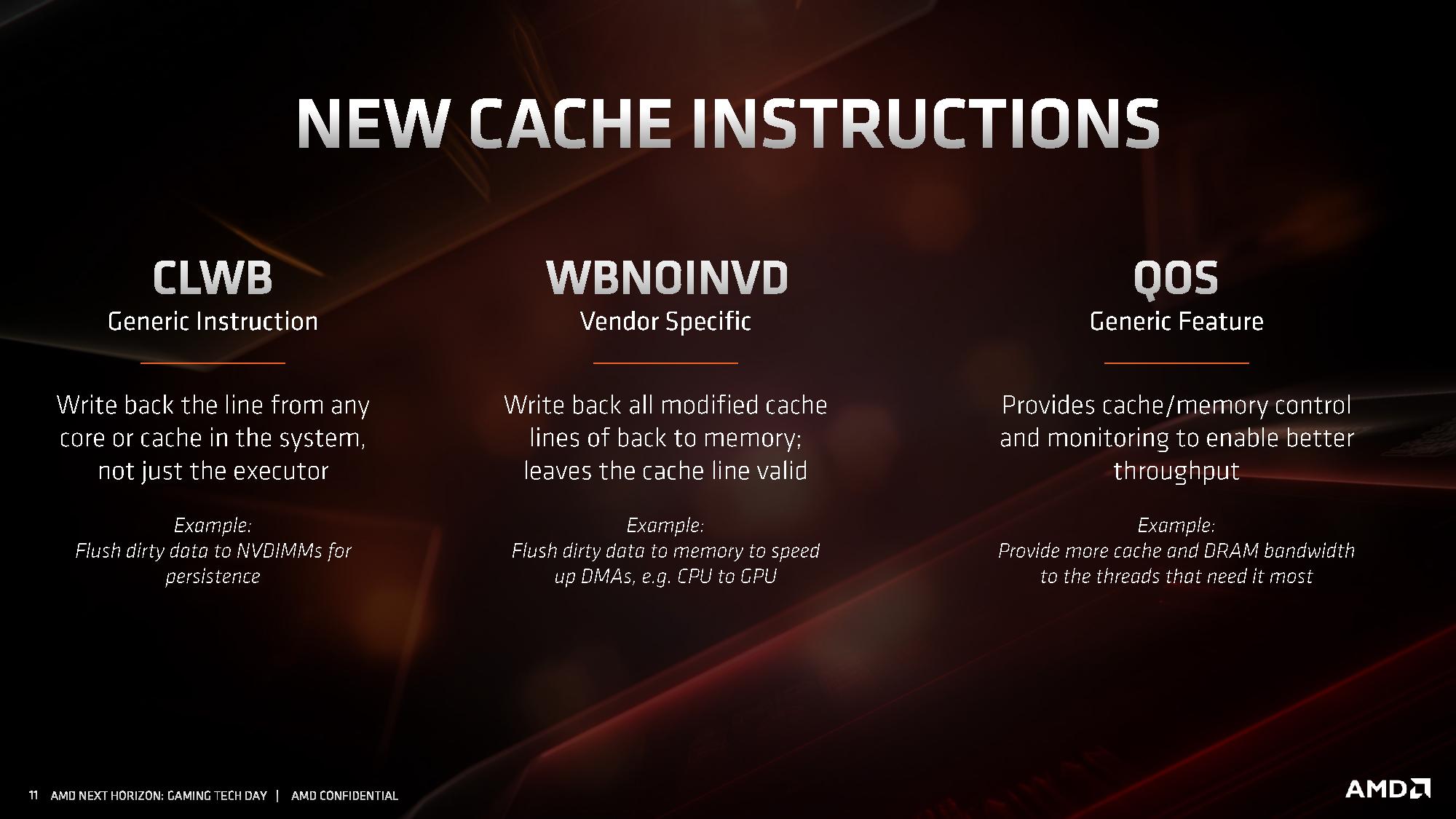
The first one, CLWB, has been seen before from Intel processors in relation to non-volatile memory. This instruction allows the program to push data back into the non-volatile memory, just in case the system receives a halting command and data might be lost. There are other instructions associated with securing data to non-volatile memory systems, although this wasn’t explicitly commented on by AMD. It could be an indication that AMD is looking to better support non-volatile memory hardware and structures in future designs, particularly in its EPYC processors.
The second cache instruction, WBNOINVD, is an AMD-only command, but builds on other similar commands such as WBINVD. This command is designed to predict when particular parts of the cache might be needed in the future, and clears them up ready in order to accelerate future calculations. In the event that the cache line needed isn’t ready, a flush command would be processed in advance of the needed operation, increasing latency – by running a cache line flush in advance while the latency-critical instruction is still coming down the pipe helps accelerate its ultimate execution.
The final set of instructions, filed under QoS, actually relates to how cache and memory priorities are assigned.
When a cloud CPU is split into different containers or VMs for different customers, the level of performance is not always consistent as performance could be limited based on what another VM is doing on the system. This is known as the ‘noisy neighbor’ issue: if someone else is eating all the core-to-memory bandwidth, or L3 cache, it can be very difficult for another VM on the system to have access to what it needs. As a result of that noisy neighbor, the other VM will have a highly variable latency on how it can process its workload. Alternatively, if a mission critical VM is on a system and another VM keeps asking for resources, the mission critical one might end up missing its targets as it doesn’t have all the resources it needs access to.
Dealing with noisy neighbors, beyond ensuring full access to the hardware as a single user, is difficult. Most cloud providers and operations won’t even tell you if you have any neighbors, and in the event of live VM migration, those neighbors might change very frequently, so there is no guarantee of sustained performance at any time. This is where a set of dedicated QoS (Quality of Service) instructions come in.
As with Intel’s implementation, when a series of VMs is allocated onto a system on top of a hypervisor, the hypervisor can control how much memory bandwidth and cache that each VM has access to. If a mission critical 8-core VM requires access to 64 MB of L3 and at least 30 GB/s of memory bandwidth, the hypervisor can control that the priority VM will always have access to that amount, and either eliminate it entirely from the pool for other VMs, or intelligently restrict the requirements as the mission critical VM bursts into full access.
Intel only enables this feature on its Xeon Scalable processors, however AMD will enable it up and down its Zen 2 processor family range, for consumers and enterprise users.
The immediate issue I had with this feature is on the consumer side. Imagine if a video game demands access to all the cache and all the memory bandwidth, while some streaming software would get access to none – it could cause havoc on the system. AMD explained that while technically individual programs can request a certain level of QoS, however it will be up to the OS or the hypervisor to control if those requests are both valid and suitable. They see this feature more as an enterprise feature used when hypervisors are in play, rather than bare metal installations on consumer systems.


216 Comments
View All Comments
Smell This - Sunday, June 16, 2019 - link
AND ...
it might be 12- to 16 IF links or, another substrate ?
Targon - Thursday, June 13, 2019 - link
Epyc and Ryzen CCX units are TSMC, the true CPU cores. The I/O unit is the only part that comes from Global Foundries, and is probably at TSMC just to satisfy the contracts currently in place.YukaKun - Monday, June 10, 2019 - link
"Users focused on performance will love the new 16-core Ryzen 9 3950X, while the processor seems nice an efficient at 65W, so it will be interesting so see what happens at lower power."Shouldn't that be 105W?
And great read as usual.
Cheers!
jjj - Monday, June 10, 2019 - link
The big problem with this platform is that ST perf per dollar gains are from zero to minimal, depending on SKU.They give us around 20% ST gains (IPC+clocks) but at a cost. Would rather have 10-15% gains for free than to pay for 20%. Pretty much all SKUs need a price drop to become exciting, some about 50$, some a bit less and the 16 cores a lot more.
Got to wonder about memory BW with the 16 cores. 2 channels with 8 cores is one thing but at 16 cores, it might become a limiting factor here and there.
Threska - Tuesday, June 11, 2019 - link
That could be said of any processor. "Yeah, drop the price of whatever it is and we'll love you for it." Improvements cost, just like DVD's costed more than VHS.jjj - Tuesday, June 11, 2019 - link
In the semi business the entire point is to offer significantly more perf per dollar every year. That's what Moore's Law was, 2x the perf at same price every 2 years. Now progress is slower but consumers aren't getting anything anymore.And in pretty much all tech driven areas, products become better every year, even cars. When there is no innovation, it means that the market is dysfunctional. AMD certainly does not innovate here, except on the balance sheet. Innovation means that you get better value and that is missing here. TSMC gives them more perf per dollar, they have additional gains from packaging but those gains do not trickle down to us. At the end of the day even Intel tries to offer 10-15% perf per dollar gains every cycle.
AlyxSharkBite - Tuesday, June 11, 2019 - link
That’s not Moore’s Law at all. It stated that the number of transistors would double. Also it’s been dead a whileSandy bridge 4c 1.16b
Coffee lake 4c is 2.1b (can’t compare the 6c or 8c)
And that’s a lot more than 2 years.
mode_13h - Tuesday, June 11, 2019 - link
Yeah, but those two chips occupy different market segments. So, you should compare Sandybridge i7 vs. Coffelake i7.Teutorix - Tuesday, June 11, 2019 - link
The number of transistors in an IC, not the number of transistors per CPU core. This is an important distinction since a CPU core in Moore's day had very little in it besides registers and an ALU. They didn't integrate FPUs until relatively recently.It's about overall transistor density, nothing more. You absolutely can compare an 8c to a 4c chip, because they are both a single IC.
An 8 core coffee lake chip is 20% smaller than a quad core sandy bridge chip. That's double the CPU cores, double the GPU cores, with probably a massive increase in the transistors/core also.
Moore's law had a minor slowdown with intel stuck at 14nm but its not dead.
Wilco1 - Tuesday, June 11, 2019 - link
Moore's Law is actually accelerating. Just not at Intel. See https://en.wikipedia.org/wiki/Transistor_count - the largest chips now have ~20 Billion transistors, and with 7nm and 5nm it looks like we're getting some more doublings soon.