AMD’s Radeon HD 6870 & 6850: Renewing Competition in the Mid-Range Market
by Ryan Smith on October 21, 2010 10:08 PM ESTBarts: The Next Evolution of Cypress
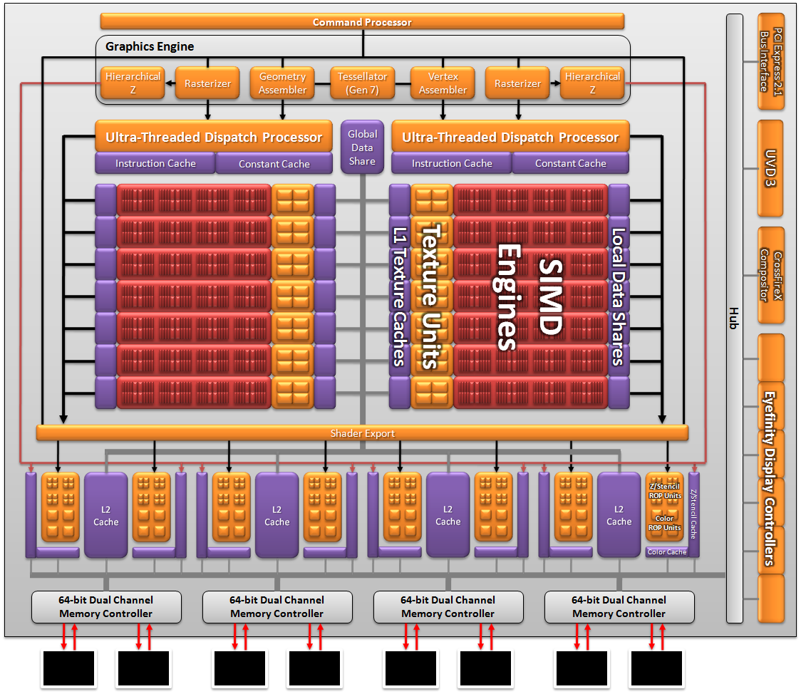
At the heart of today’s new cards is Barts, the first member of AMD’s Northern Island GPUs. As we quickly hinted at earlier, Barts is a very direct descendant of Cypress. This is both a product of design, and a product of consequences.
It should come as no surprise that AMD was originally looking to produce what would be the Northern Islands family on TSMC’s 32nm process; as originally scheduled this would line up with the launch window AMD wanted, and half-node shrinks are easier for them than trying to do a full-node shrink. Unfortunately the 32nm process quickly became doomed for a number of reasons.
Economically, per-transistor it was going to be more expensive than the 40nm process, which is a big problem when you’re trying to make an economical chip like Barts. Technologically, 32nm was following TSMC’s troubled 40nm process; TSMC’s troubles ended up being AMD’s troubles when they launched the 5800 series last year, as yields were low and wafers were few, right at a time where AMD needed every chip they could get to capitalize on their lead over NVIDIA. 32nm never reached completion so we can’t really talk about yields or such, but it’s sufficient to say that TSMC had their hands full fixing 40nm and bringing up 28nm without also worrying about 32nm.
Ultimately 32nm was canceled around November of last year. But even before that AMD made the hard choice to take a hard turn to the left and move what would become Barts to 40nm. As a result AMD had to make some sacrifices and design choices to make Barts possible on 40nm, and to make it to market in a short period of time.
For these reasons, architecturally Barts is very much a rebalanced Cypress, and with the exception of a few key changes we could talk about Barts in the same way we talked about Juniper (the 5700 series) last year.
Click to enlarge
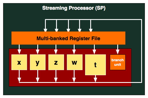
Barts continues AMD’s DirectX 11 legacy, building upon what they’ve already achieved with Cypress. At the SPU level, like Cypress and every DX10 AMD design before it continues to use AMD’s VLIW5 design. 5 stream processors – the w, x, y, z, and t units – work together with a branch unit and a set of GPRs to process instructions. The 4 simple SPs can work together to process 4 FP32 MADs per clock, while the t unit can either do FP32 math like the other units or handle special functions such as a transcendental. Here is a breakdown of what a single Barts SPU can do in a single clock cycle:
- 4 32-bit FP MAD per clock
- 4 24-bit Int MUL or ADD per clock
- SFU : 1 32-bit FP MAD per clock
Compared to Cypress, you’ll note that FP64 performance is not quoted, and this isn’t a mistake. Barts isn’t meant to be a high-end product (that would be the 6900 series) so FP64 has been shown the door in order to bring the size of the GPU down. AMD is still a very gaming-centric company versus NVIDIA’s philosophy of GPU computing everywhere, so this makes sense for AMD’s position, while NVIDIA’s comparable products still offer FP64 if only for development purposes.
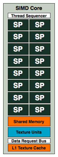
Above the SPs and SPUs, we have the SIMD. This remains unchanged from Cypress, with 80 SPs making up a SIMD. The L1 cache and number of texture units per SIMD remains at 16KB L1 texture, 8KB L1 compute, and 4 texture units per SIMD.
At the macro level AMD maintains the same 32 ROP design (which combined with Barts’ higher clocks, actually gives it an advantage over Cypress). Attached to the ROPs are AMD’s L2 cache and memory controllers; there are 4 128KB blocks of L2 cache (for a total of 512KB L2) and 4 64bit memory controllers that give Barts a 256bit memory bus.
Barts is not just a simple Cypress derivative however. For non-gaming/compute uses, UVD and the display controller have both been overhauled. Meanwhile for gaming Barts did receive one important upgrade: an enhanced tessellation unit. AMD has responded to NVIDIA’s prodding about tessellation at least in part, equipping Barts with a tessellation unit that in the best-case scenario can double their tessellation performance compared to Cypress. AMD has a whole manifesto on tessellation that we’ll get in to, but for now we’ll work with the following chart:
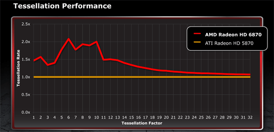
AMD has chosen to focus on tessellation performance at lower tessellation factors, as they believe these are the most important factors for gaming purposes. From their own testing the advantage over Cypress approaches 2x between factors 6 and 10, while being closer to a 1.5x increase before that and after that up to factor 13 or so. At the highest tessellation factors Barts’ tessellation unit falls to performance roughly in line with Cypress’, squeezing out a small advantage due to the 6870’s higher clockspeed. Ultimately this means tessellation performance is improved on AMD products at lower tessellation factors, but AMD’s tessellation performance is still going to more-or-less collapse at high factors when they’re doing an extreme amount of triangle subdivision.
So with all of this said, Barts ends up being 25% smaller than Cypress, but in terms of performance we’ve found it to only be 7% slower when comparing the 6870 to the 5870. How AMD accomplished this is the rebalancing we mentioned earlier.
Based on AMD’s design decisions and our performance data, it would appear that Cypress has more computing/shading power than it necessarily needs. True, Barts is slower, but it’s a bit slower and a lot smaller. AMD’s various compute ratios, such as compute:geometry and compute:rasterization would appear to be less than ideal on Cypress. So Barts changes the ratios.
Compared to Cypress and factoring in 6870/5870 clockspeeds, Barts has about 75% of the compute/shader/texture power of Cypress. However it has more rasterization, tessellation, and ROP power than Cypress; or in other words Barts is less of a compute/shader GPU and a bit more of a traditional rasterizing GPU with a dash of tessellation thrown in. Even in the worst case scenarios from our testing the drop-off at 1920x1200 is only 13% compared to Cypress/5870, so while Cypress had a great deal of compute capabilities, it’s clearly difficult to make extremely effective use of it even on the most shader-heavy games of today.
However it’s worth noting that internally AMD was throwing around 2 designs for Barts: a 16 SIMD (1280 SP) 16 ROP design, and a 14 SIMD (1120 SP) 32 ROP design that they ultimately went with. The 14/32 design was faster, but only by 2%. This along with the ease of porting the design from Cypress made it the right choice for AMD, but it also means that Cypress/Barts is not exclusively bound on the shader/texture side or the ROP/raster side.
Along with selectively reducing functional blocks from Cypress and removing FP64 support, AMD made one other major change to improve efficiency for Barts: they’re using Redwood’s memory controller. In the past we’ve talked about the inherent complexities of driving GDDR5 at high speeds, but until now we’ve never known just how complex it is. It turns out that Cypress’s memory controller is nearly twice as big as Redwood’s! By reducing their desired memory speeds from 4.8GHz to 4.2GHz, AMD was able to reduce the size of their memory controller by nearly 50%. Admittedly we don’t know just how much space this design choice saved AMD, but from our discussions with them it’s clearly significant. And it also perfectly highlights just how hard it is to drive GDDR5 at 5GHz and beyond, and why both AMD and NVIDIA cited their memory controllers as some of their biggest issues when bringing up Cypress and GF100 respectively.
Ultimately all of these efficiency changes are necessary for AMD to continue to compete in the GPU market, particularly in the face of NVIDIA and the GF104 GPU powering the GTX 460. Case in point, in the previous quarter AMD’s graphics division only made $1mil in profit. While Barts was in design years before that quarter, the situation still succinctly showcases why it’s important to target each market segment with an appropriate GPU; harvested GPUs are only a stop-gap solution, in the end purposely crippling good GPUs is a good way to cripple a company’ s gross margin.


197 Comments
View All Comments
Ryan Smith - Friday, October 22, 2010 - link
Quality is unchanged. UVD 3 adds a few fixed function blocks, but quality is a matter of post-processing and hence affected by the drivers once you have sufficient shader power to do all the post-processing.Pastuch - Friday, October 22, 2010 - link
I posted about this earlier but my post was deleted.Ryan there is a ton of HTPC users on this site.
1. Exactly how long is the Radeon 6870/6850 vs the GTX 460?
2. How does the GTX460 compare to the Radeon 6 series regarding bitstreaming high def audio?
3. How UVD3 post-processing compare to Nvidias?
Ryan Smith - Friday, October 22, 2010 - link
It's exactly the same as this: http://www.anandtech.com/show/3973/nvidias-geforce...HigherGround - Friday, October 22, 2010 - link
Why was EVGA card included in this test? The rest of the field is generic (non OC, no brand), so why included an OC card, which skews the readers perspective? Pretty sure EVGA paid you to included its top OC card in this review ...Parhel - Friday, October 22, 2010 - link
No, NVidia paid them to include it. NVidia sends "guidelines" to all the hardware review sites, telling them what settings to use and which cards to use in the comparison. In the guidelines for today's review was to use the EVGA GTX 460 FTW, and and site you see using it is essentially a paid NVidia shill.I could care less about ATI vs NVidia, as I'm not really a gamer, but I'm very disappointed today to see my long time favorite hardware site stooping to this level. In the end, it gives consumers bad information, which should be antithetical to the purpose of a site like this.
AtwaterFS - Friday, October 22, 2010 - link
I agree, this site is typically class-leading, but this article give AnandTech a bit of a black eye and the results dont particularly jive with "un-biased" sites like HardOCP.DrKlahn - Friday, October 22, 2010 - link
I was going to post the same thing. As a long time reader of this site, I was very disappointed with the decision to include the overclocked card. Either the ATI cards should have been overclocked and their results provided in every test or it should have been excluded as per the normal benchmarking guidelines.I would have no issue with a followup or side article comparing factory overclocked offerings. But this is clearly bowing to pressure from Nvidia and I expected better of this site.
aungee - Saturday, October 23, 2010 - link
To Include the EVGA GTX 460 FTW was unfair and whether intentional or not it did spoil the launch party for AMD on this site to some degree. It would have been more appropriate to make a small mention of it's existence and to benchmark it in the future against any factory OC 6800 cards.After getting your head around the naming, AMD needs to be credited for bringing such a performance on only a 255 mm2 package (it even caused the price drop for the 530mm2 GTX 470) . AMD has headroom to drop the price of the 6800 cards so lets hope they do soon.
tigersty1e - Friday, October 22, 2010 - link
I couldn't find the clocks, but if you do include an OC'd card in your benches, you should give us the clocks.dertechie - Friday, October 22, 2010 - link
850 MHz Core, 1700 MHz shaders, 4 GHz Memory, up from 675 MHz Core, 1350 MHz shaders, 3.6 GHz Memory.That's a 26% Core OC and an 11% Memory OC. However, the cost has been OC'd too, the FTW card costs the same $240 as the stock Radeon 6870.