NVIDIA's Tegra 3 Launched: Architecture Revealed
by Anand Lal Shimpi on November 9, 2011 12:34 AM ESTThe Tegra 3 GPU: 2x Pixel Shader Hardware of Tegra 2
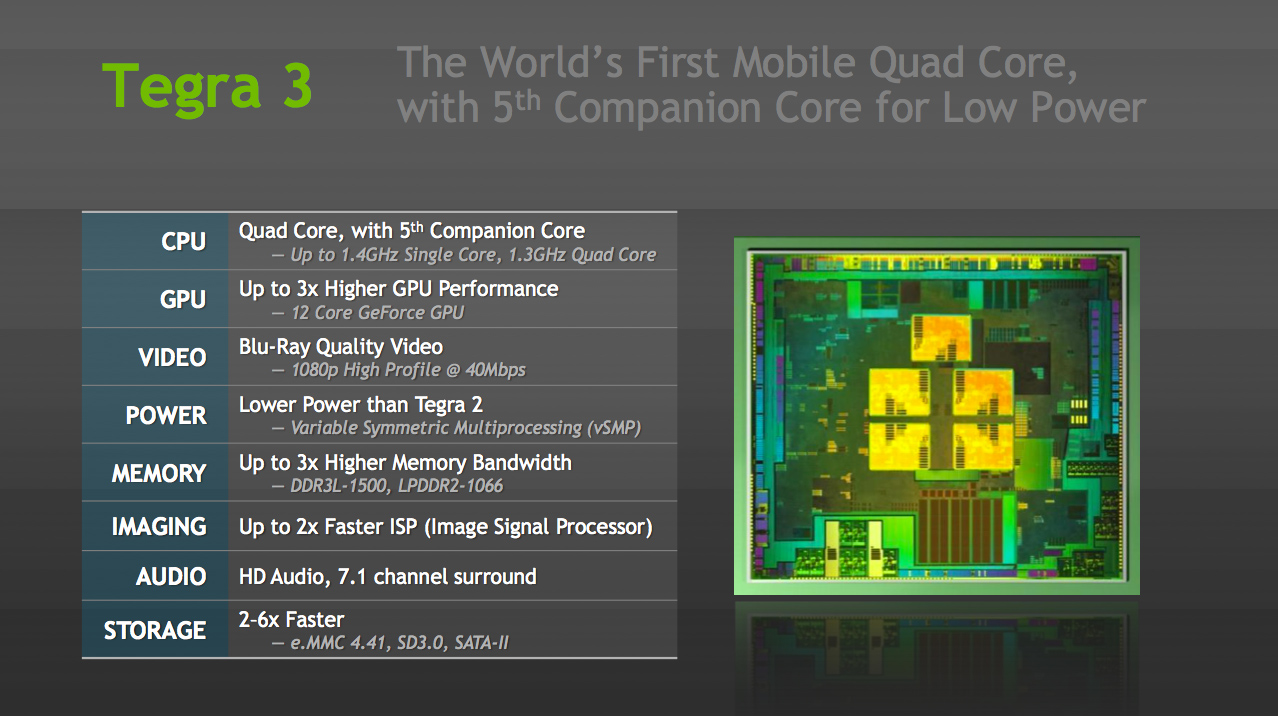
Tegra 3's GPU is very much an evolution of what we saw in Tegra 2. The GeForce in Tegra 2 featured four pixel shader units and four vertex shader units; in Tegra 3 the number of pixel shader units doubles while the vertex processors remain unchanged. This brings Tegra 3's GPU core count up to 12. NVIDIA still hasn't embraced a unified architecture, but given how closely it's mimicking the evolution of its PC GPUs I wouldn't expect such a move until the next-gen architecture - possibly in Wayne.
| Mobile SoC GPU Comparison | |||||||||||
| Adreno 225 | PowerVR SGX 540 | PowerVR SGX 543 | PowerVR SGX 543MP2 | Mali-400 MP4 | GeForce ULP | Kal-El GeForce | |||||
| SIMD Name | - | USSE | USSE2 | USSE2 | Core | Core | Core | ||||
| # of SIMDs | 8 | 4 | 4 | 8 | 4 + 1 | 8 | 12 | ||||
| MADs per SIMD | 4 | 2 | 4 | 4 | 4 / 2 | 1 | 1 | ||||
| Total MADs | 32 | 8 | 16 | 32 | 18 | 8 | 12 | ||||
| GFLOPS @ 200MHz | 12.8 GFLOPS | 3.2 GFLOPS | 6.4 GFLOPS | 12.8 GFLOPS | 7.2 GFLOPS | 3.2 GFLOPS | 4.8 GFLOPS | ||||
| GFLOPS @ 300MHz | 19.2 GFLOPS | 4.8 GFLOPS | 9.6 GFLOPS | 19.2 GFLOPS | 10.8 GFLOPS | 4.8 GFLOPS | 7.2 GFLOPS | ||||
Per core performance has improved a bit. NVIDIA worked on timing of critical paths through the GPU's execution units to help it run at higher clock speeds. NVIDIA wouldn't confirm the target clock for Tegra 3's GPU other than to say it was higher than Tegra 2's 300MHz. Peak floating point throughput per core is unchanged (one MAD per clock), but each core should be more efficient thanks to larger caches in the design.
A combination of these improvements as well as newer drivers are what give Tegra 3's GPU its 2x - 3x performance advantage over Tegra 2 despite only a 50% increase in overall execution resources. In pixel shader bound scenarios, there's an effective doubling of execution horsepower so the 2x gains are more believable there. I don't expect many games will be vertex processing bound so the lack of significant improvement there shouldn't be a big issue for Tegra 3.
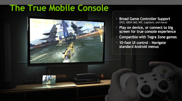
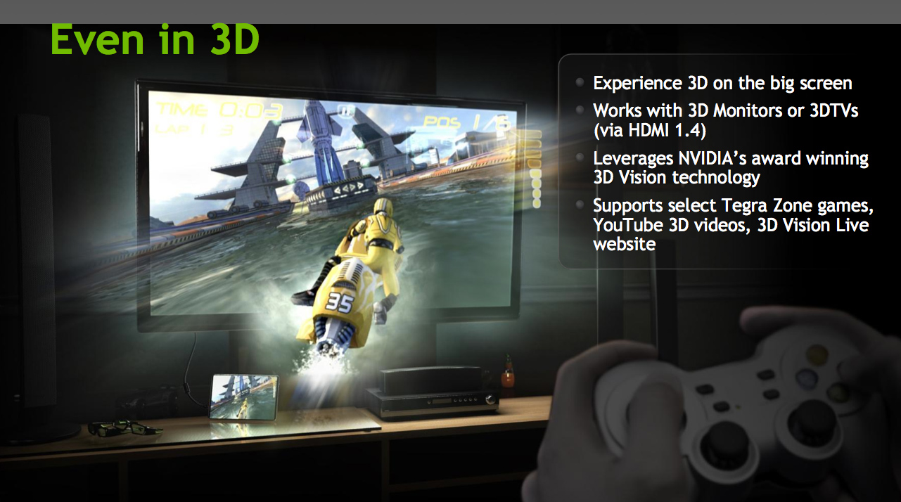
Ready for Gaming: Stereoscopic 3D and Expanded Controller Support
Tegra 3 now supports stereoscopic 3D for displaying content from YouTube, NVIDIA's own 3D Vision Live website and some Tegra Zone games. In its port of Android, NVIDIA has also added expanded controller support for PS3, Xbox 360 and Wii controllers among others.
Tegra 3 Video Encoding/Decoding and ISP
There's unfortunately not too much to go on here, especially not until we have some testable hardware in hand, but NVIDIA is claiming a much improved video decoder and more efficient video encoder in Tegra 3.
Tegra 3's video decoder can accelerate 1080p H.264 high profile content at up to 40Mbps, although device vendors can impose their own bitrate caps and file limitations on the silicon. NVIDIA wouldn't go into greater detail as to what's changed since Tegra 2, other than to say that the video decoder is more efficient. The video encoder is capable of 1080p H.264 base profile encode at 30 fps.
The Image Signal Processor (ISP) in Tegra 3 is twice as fast as what was in Tegra 2 and NVIDIA promised more details would be forthcoming (likely alongside the first Tegra 3 smartphone announcements).
Memory Interface: Still Single Channel, DDR3L-1500 Supported
Tegra 3 supports higher frequency memories than Tegra 2 did, but the memory controller itself is mostly unchanged from the previous design. While Tegra 2 supported LPDDR2 at data rates of up to 600MHz, Tegra 3 increases that to LPDDR2-1066 and DDR3-L is supported at data rates of up to 1500MHz. The memory interface is still only 32-bits wide, resulting in far less theoretical bandwidth than Apple's A5, Samsung's Exynos 4210, TI's OMAP 4, or Qualcomm's upcoming MSM8960. This is particularly concerning given the increase in core count as well as GPU execution resources. NVIDIA doesn't expect memory bandwidth to be a limitation, but I can't see how that wouldn't be the case in 3D games. Perhaps it's a good thing that Infinity Blade doesn't yet exist for Android.
SATA II Controller: On Die
Given Tegra 3 will find itself in convertible Windows 8 tablets, this next feature makes a lot of sense. NVIDIA's latest SoC includes an on-die SATA II controller, a feature that wasn't present on Tegra 2.


94 Comments
View All Comments
psychobriggsy - Friday, November 11, 2011 - link
By using 40nm NVIDIA has achieved a first to market advantage in the high-end quad-core SoC for tablets. Obviously this comes at the cost of a larger die, higher power consumption and/or slower clock speeds.The larger die will add some cost to the product, but it's hardly a problem given that it is still quite small in the grand scheme of things. I believe it is smaller than the A5 for example. In addition mature yields on the 40nm process may allow NVIDIA to ship millions without worry rather than risk early 28nm yields.
Tegra 3 was meant to clock to over 1.5GHz, and this hasn't been achieved, probably 1.3GHz was the better option for power consumption. 28nm will fix this for Tegra 3+ next year, hopefully.
In addition the low power core gives NVIDIA an early entry into the low-power companion core market a year or two before the ARM Cortex A15 + ARM Cortex A7 combos arrive. This is another reason it is 40nm - TSMC don't have the ability to fab 28nm dies with a combination of processes (LP and HP) on the same die yet.
So the die might costs a couple of dollers more to make vs Tegra 2, but I'm sure they can charge a premium for the product until the competitors arrive.
Paulman - Wednesday, November 9, 2011 - link
Wow, I'm amazed by the response times. It looks pretty seamless (i.e. the switching to and from the low-power transistor companion core). From a GUI perspective, there doesn't appear to be any stutter at all.Looks like a good job, NVIDIA :O
P.S. Speaking of low-power transistors, that's ingenious to build an entire core out of low-power transistors on the same die as the four regular cores. I wonder if that's an idea that's been floating around in the field for awhile...
dagamer34 - Wednesday, November 9, 2011 - link
You think using LP transistors is something, see big.LITTLE coming from ARM in 2012-2013. ARM designed an entire core to be specifically low power (the Cortex A7) to fit perfectly with the more powerful Cortex A15, so that you get even greater performance with even greater power savings.Mugur - Wednesday, November 9, 2011 - link
Yes, but Tegra 3 is already here...Draiko - Wednesday, November 9, 2011 - link
It seems like nVidia and ARM co-developed this kind of Architecture. nVidia is implementing it in the Tegra 3 and ARM is making it available for license with bigLITTLE.I'm just blown away with how smooth the dynamic threading is on the Tegra 3. This is going to be an absolute game-changer.
JonnyDough - Wednesday, November 9, 2011 - link
That's because it isn't loaded down with crapware like the Blockbuster app...yet.metafor - Wednesday, November 9, 2011 - link
IIRC, Marvell's Sheeva processors uses this method (came out ~2010 I believe).jcompagner - Thursday, November 10, 2011 - link
intel does this also for quite some timeWas the SATA bug they had not a result of something like this?
There also there was a wrong type of transistor used for that.
Omega215D - Wednesday, November 9, 2011 - link
Seeing that the architecture has a sound processor in it, is there any chance that nVidia could revive SoundStorm for the mobile platform? That would be great for things like the Transformer and other tablets as well as smart phones for multimedia purposes. Just a thought.ggathagan - Wednesday, November 9, 2011 - link
Given the Tegra 3 already includes HD audio and 7.1 support, I'm not clear on what feature you think Soundstream would add.