Understanding Camera Optics & Smartphone Camera Trends, A Presentation by Brian Klug
by Brian Klug on February 22, 2013 5:04 PM EST- Posted in
- Smartphones
- camera
- Android
- Mobile
The Imaging Chain
Since we’re talking about a smartphone we must understand the imaging chain, and thus block diagram, and how the blocks work together. There’s a multiplicative effect on quality as we move through the system from left to right. Good execution on the optical system can easily be mitigated away by poor execution on the ISP for example. I put arrows going left to right from some blocks since there’s a closed loop between ISP and the rest of the system.

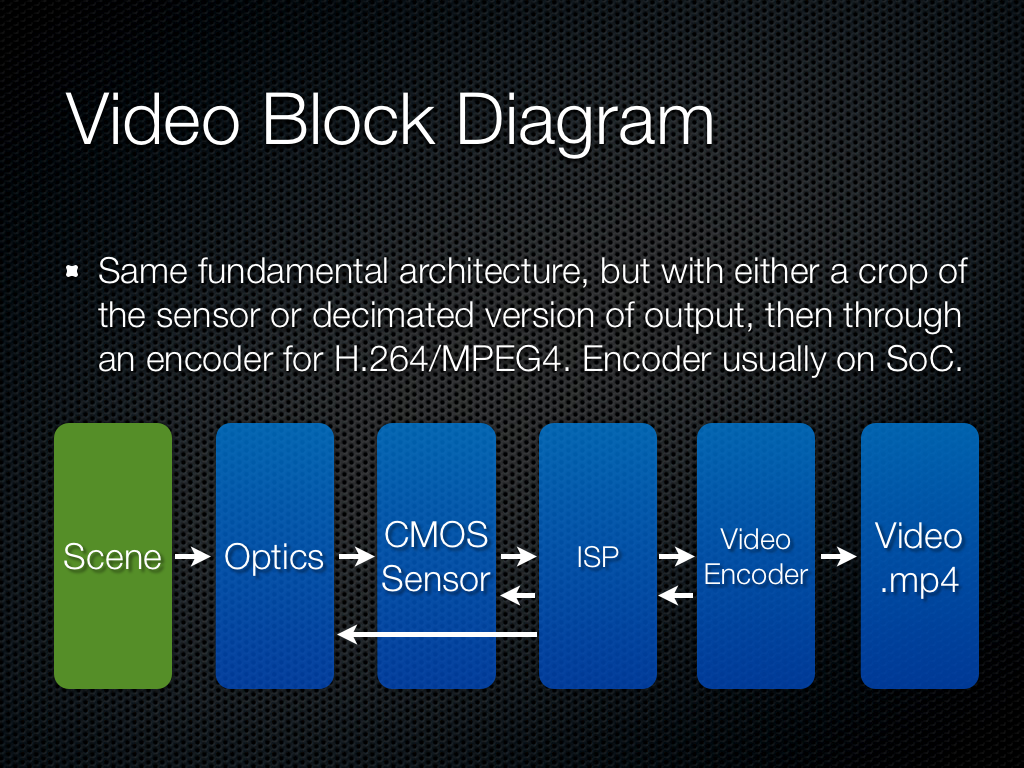
The video block diagram is much the same, but includes an encoder in the chain as well.
Smartphone Cameras: The Constraints
The constraints for a smartphone camera are pretty unique, and I want to emphasize just how much of a difficult problem this is for OEMs. Industrial design and size constraints are pretty much the number one concern — everyone wants a thin device with no camera bump or protrusion, which often leaves the camera module the thickest part of the device. There’s no getting around physics here unfortunately. There’s also the matter of cost, since in a smartphone the camera is just one of a number of other functions. Material constraints due to the first bullet point and manufacturing (plastic injection molded aspherical shapes) also makes smartphone optics unique. All of this then has to image onto tiny pixels.
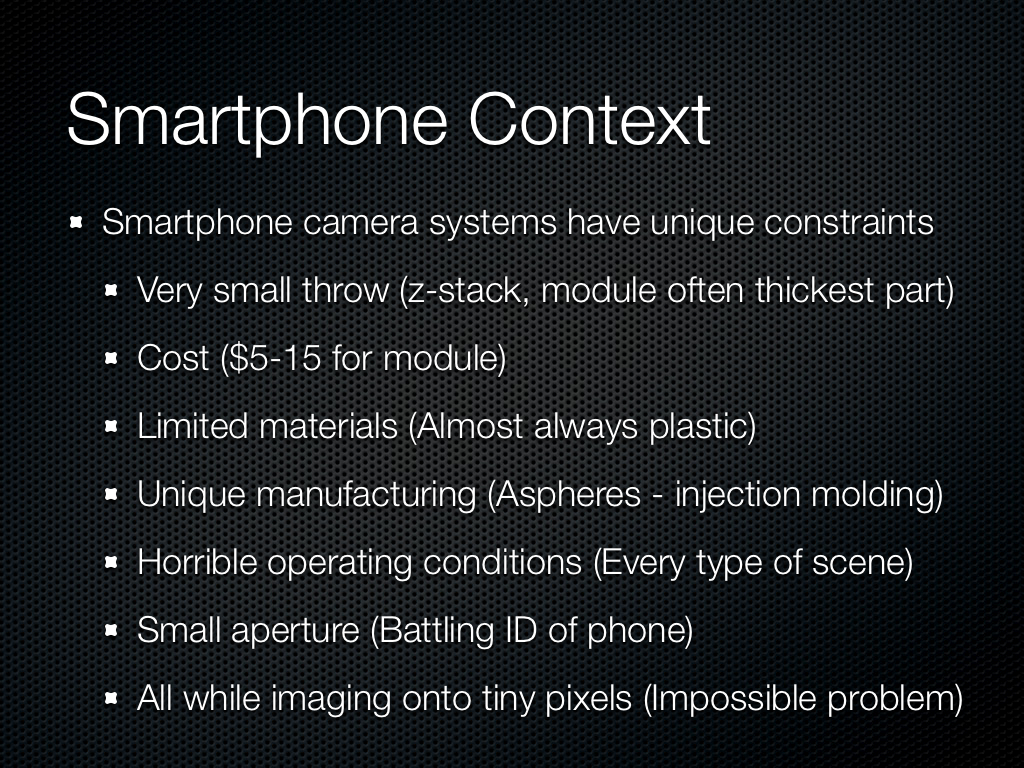
Starting with the first set of constraints are material choices. Almost all smartphone camera modules (excluding some exceptions from Nokia) the vast majority of camera optics that go into a tiny module are plastic. Generally there are around 2 to 5 elements in the system, and you’ll see a P afterwards for plastic. There aren’t too many optical plastics around to chose from either, but luckily enough one can form a doublet with PMMA as something of a crown (low dispersion) and Polystyrene as a flint (high dispersion) to cancel chromatic aberration. You almost always see some doublet get formed in these systems. Other features of a smartphone are obvious but worth stating, they almost always are fixed focal length, fixed aperture, with no shutter, sometimes with an ND filter (neutral density) and generally not very low F-number. In addition to keep modules thin, focal length is usually very short, which results in wide angle images with lots of distortion. Ideally I think most users want something between 35 mm or 50 mm in 35mm equivalent numbers.
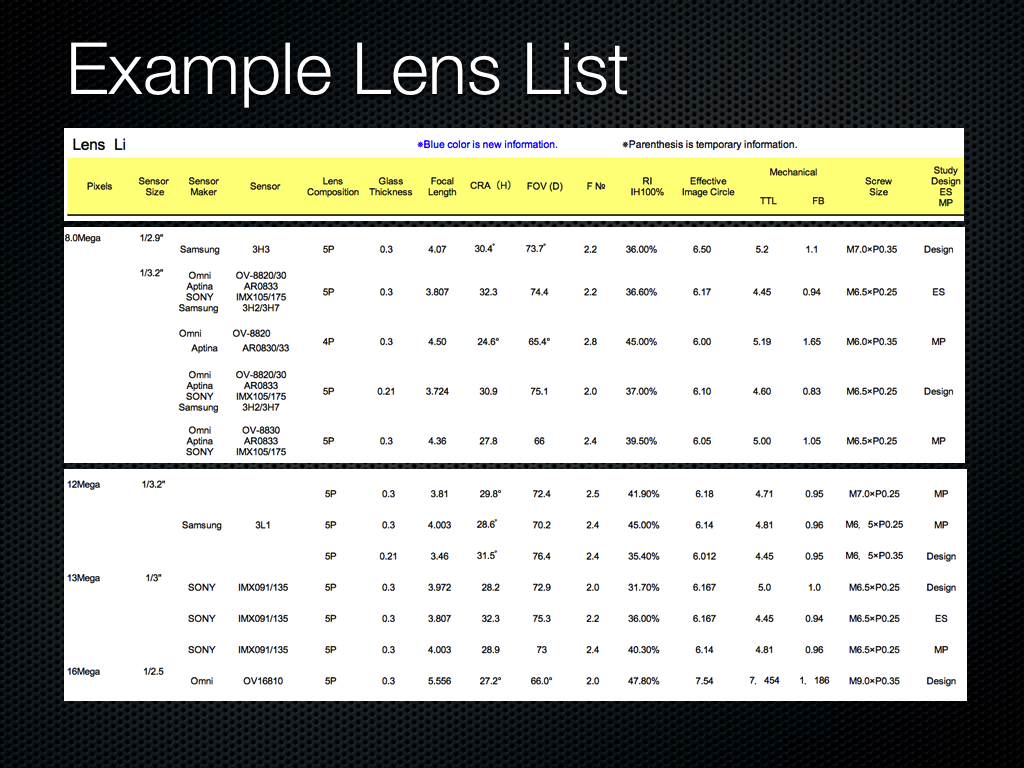
I give an example lens catalog from a manufacturer, you can order these systems premade and designed to a particular sensor. We can see the different metrics of interest, thickness, chief ray angle, field of view, image circle, thickness, and so on.
During undergrad a typical homework problem for optical design class would include a patent lens, and then verification of claims about performance. Say what you want about the patent system, but it’s great for getting an idea about what’s out there. I picked a system at random which looks like a front facing smartphone camera system, with wide field of view, F/2.0, and four very aspherical elements.
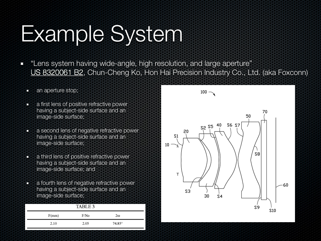
Inside a patent is a prescription for each surface, and the specification here is like almost all others in format. The radius of curvature for each surface, distance between surfaces, index, abbe number (dispersion), and conic constant are supplied. We can see again lots of very aspherical surfaces. Also there’s a doublet right for the first and second element (difference in dispersion and positive followed by negative lens) to correct some chromatic aberrations.

What do these elements look like? Well LG had a nice breakdown of the 5P system used in its Optimus G, and you can see just what the lenses in the system look like.


60 Comments
View All Comments
ssj3gohan - Sunday, February 24, 2013 - link
Couple of comments on this and your rant in the podcast :)First of all, you're lauding HTC for their larger pixel size and lamenting the move towards smaller pixels. But isn't it true that effective resolution, especially when your pixels are significantly smaller than the airy disk, is basically a function of integration area? The only downside to using smaller pixels is that you increase the effect of read noise and decrease fill factor. In an ideal world, a 100MP phone camera with the same sensor size as a 10MP one would make pictures that are just as good. With read noise being essentially absent nowadays, I don't see the reason to particularly bash on 13MP phone cameras compared to larger-pixel but same-integration-area sensors. They make the same pictures, just take up a little less space on the sd card.
Of course, you could make the argument that it's wrong to give in to the 'moar megapixels!' consumer side of things and try to educate people that sometimes less is more.
Next, you say that refractive index and focal length is essentially what limits the focal length for very thin cameras, but this can be alleviated by using diffractive optics (not yet now, but in the future). We may very well see 3mm-thickness 35mm focal length equivalent camera modules with large sensors someday. It's technically possible. Especially with, as you said, nanodiamonds and other very high refractive index synthetic lens materials in the making.
Next, about the resolving power. There's the airy disk and rayleigh's criterion, but this is not the end of resolving power. It does make sense to oversample beyond this point, you will get extra image information. It becomes exponentially less as you increase the megapixel count but you can still get about 150% extra image information by oversampling beyond the size of the airy disk. Again, in an ideal world without drawbacks to doing so, this does make sense.
tuxRoller - Sunday, February 24, 2013 - link
Especially, with the use of metamaterials that make use of negative indexes of refraction to allow you to resolve detail beyond the diffraction limit?ssj3gohan - Monday, February 25, 2013 - link
Well, keep in mind that the reason you can resolve beyond the diffraction limit is the fact that the geometrical properties of the sensor and optics differ. Optics will by definition cause gaussian blur as their defect mode, while the sensor has square and offset pixels. These areas do not overlap perfectly, so in order to perfectly image that blurry optical image you need pixels that are smaller than the fundamental size of the diffraction pattern (airy disk).These optical effects don't go away when you're using metamaterials/quantum opticss/etc. Light will still be a wave that will not necessarily enter the sensor perfectly perpendicular.
UltraTech79 - Monday, February 25, 2013 - link
I ave seen many many reviews of lenses and the technical details of digital imaging ect, and almost every time the article would have really shitty JPG images. I found it highly ironic. Kudos to you for using PNG throughout this quality article.AnnihilatorX - Monday, February 25, 2013 - link
I was reading the review for Sony's Xperia Z at techradar, I was astonished at how poor the 13MP Exmor RS sensor performs. Frankly, the image looks blurry and more like it's taken by a 5MP scaled up, with heavy noise even in a well lit scene:http://mos.futurenet.com/techradar/art/mobile_phon...
While I don't really care too much about smart phone camera, and I use my budget DSLR (cheaper than a smart phone) for my photography pleasure, I was thinking if the MP race and new gen smart phones can eliminate the need for me to lunge a DSLR around. If this article is correct on the physical limitations of smartphone camera technology, looks like there is still a future for DSLRs.
danacee - Monday, February 25, 2013 - link
Traditional, aka -crap- P&S clearly are at a disadvantage now, only the still very useful of optical zoom keeping them alive. However high end, 'big' sensor P&S such as the not too young Sony RX100 are still many many generations ahead of smartphone cameras, even the Nokia Pureview has terrible image quality next to it.pandemonium - Tuesday, February 26, 2013 - link
I am surprised at the lack of mention for Carl Zeiss lenses in here. If you're going to make an article about lens quality and cameraphone technology, why wouldn't you include the best in the market for such? Or are we disputing that fact?Also, not all cameraphones suffer as much from dramatic lens flare discoloration issues as said "very popular phone."
ShieTar - Tuesday, February 26, 2013 - link
Sure, you get a 3µm diffraction spot on your camera, and with 1.1µm pixels it gets oversampled. But that does not have to be a waste. As long as the diffraction pattern is well characterised, you can remove the diffraction effect through a deconvolution as part of your ISP. This even remains true for near-field optical effects that occur once you pixel size gets close to or below the image wavelength. As long as such corrections are implemented, and as long as your per-pixel noise is small enough for these algorithms to work, decreasing the pixel size does make a certain sense.Once noise becomes a larger problem then resolution, the smaller pixels hurt though, by wasting light through the larger crop factor and also by increasing the overall read-out noise. When exactly that point is reached depends on the light conditions you want to use your camera in, so it would be interesting to understand for which kind of conditions smartphone-cameras are being optimised.
rwei - Wednesday, February 27, 2013 - link
hurr hurrtheSuede - Wednesday, February 27, 2013 - link
I don't know where your Rayleigh limit comes from, but in real world optics, Rayleigh is:[1.22 x F# x wavelength] -giving 1.3µm for green (550nm) light in an F2.0 lens.
But maybe it's your interpretation of Rayleigh that is wrong, and that's where the error stems from. From the graphs, you show spot resolution limit as 2xRayleigh - and it isn't. Spot resolution is 1xRayleigh - giving an F2.0 lens a maximum resolution of the aforementioned 1.3µm - NOT 2.6µm.
The definition of Rayleigh:
-"Two point sources are regarded as just resolved when the principal diffraction maximum of one image coincides with the first minimum of the other.
"Just resolved" in this case means a resulting MTF of about 7% - i.e The minimum distance between two peaks where you can still resolve that they are two, not one large is equal to the RADIUS of the first null on the Airy disk. Not the diameter. This is quite a common error made by people from the "E" side of ElectrOptics.