The MSI HQ Tour: Design 101
by Ian Cutress on July 7, 2015 8:00 AM EST- Posted in
- Motherboards
- MSI
- Trade Shows
- Notebooks
- HQ
- Tour
- Computex 2015
As with the other manufacturers we have visited, a substantial amount of internal testing has to be performed in order to satisfy regulations in the countries that sell the products but also when we’re discussing compatibility. The motherboard side of this is the most stringent, as users can plug any number of devices in but if the implementation is not correct then sometimes workarounds or extra code has to be added to compensate.
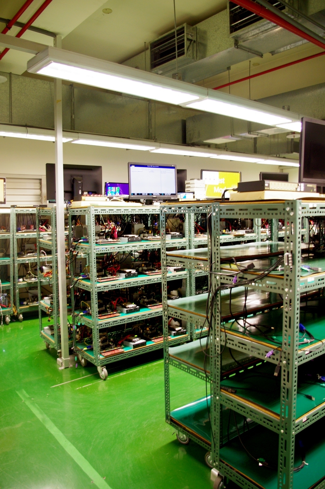
Thus as expected we get a bulk testing room like this, filled with racks of motherboards stress testing DRAM, graphics cards, SSDs and others. Obviously each motherboard design and revision needs to pass the tests here.
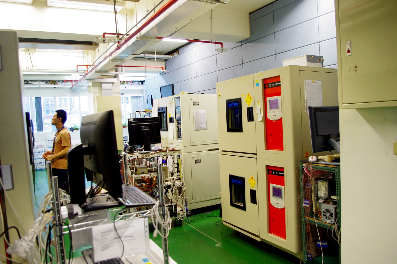
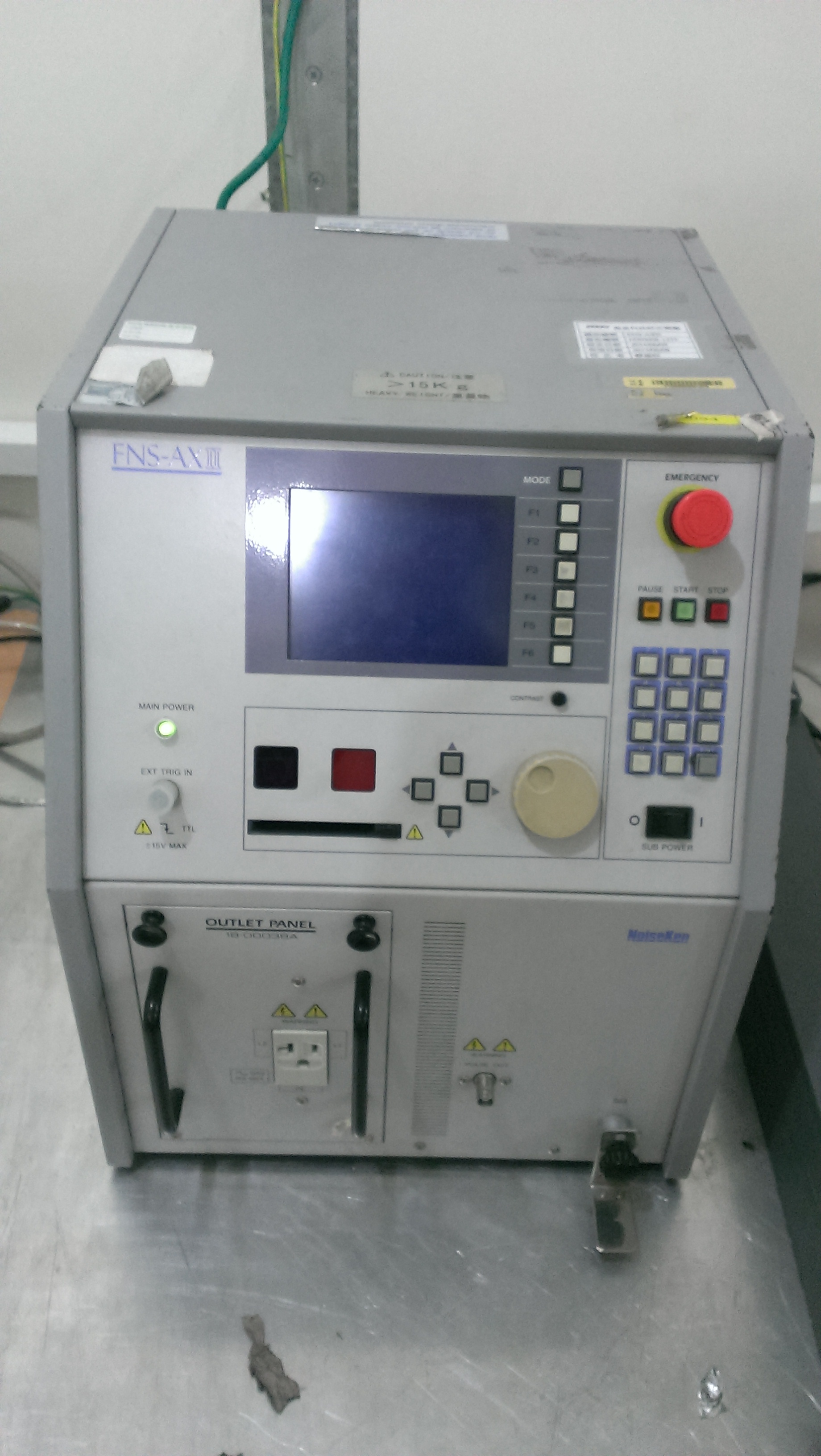
MSI’s focus on military class certification is a cornerstone of the brand. The official certification requires tests being performed offsite, but internally MSI has to ensure that its products will pass those tests. As a result, we get heat and cold testing facilities here, processing through a range of temperatures.
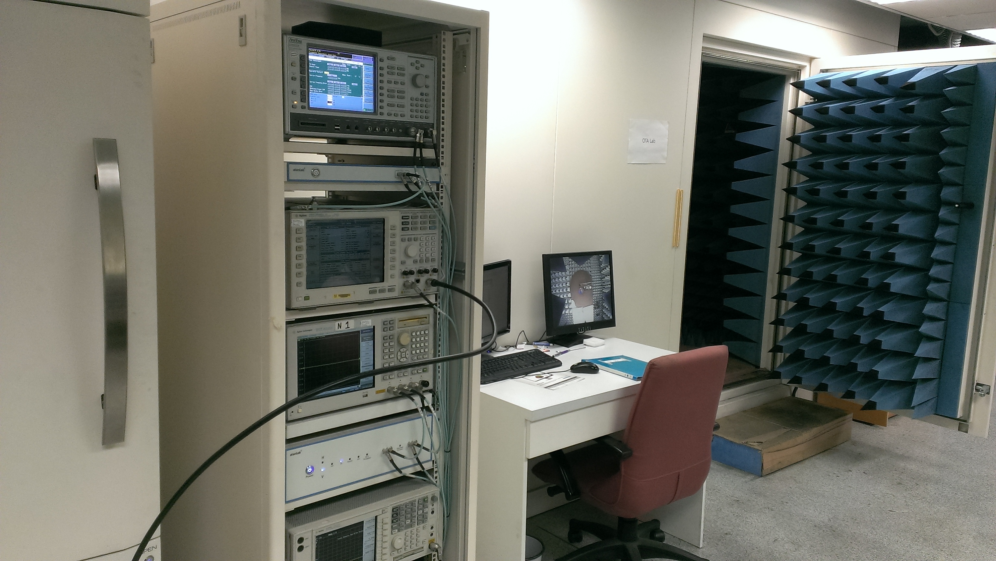
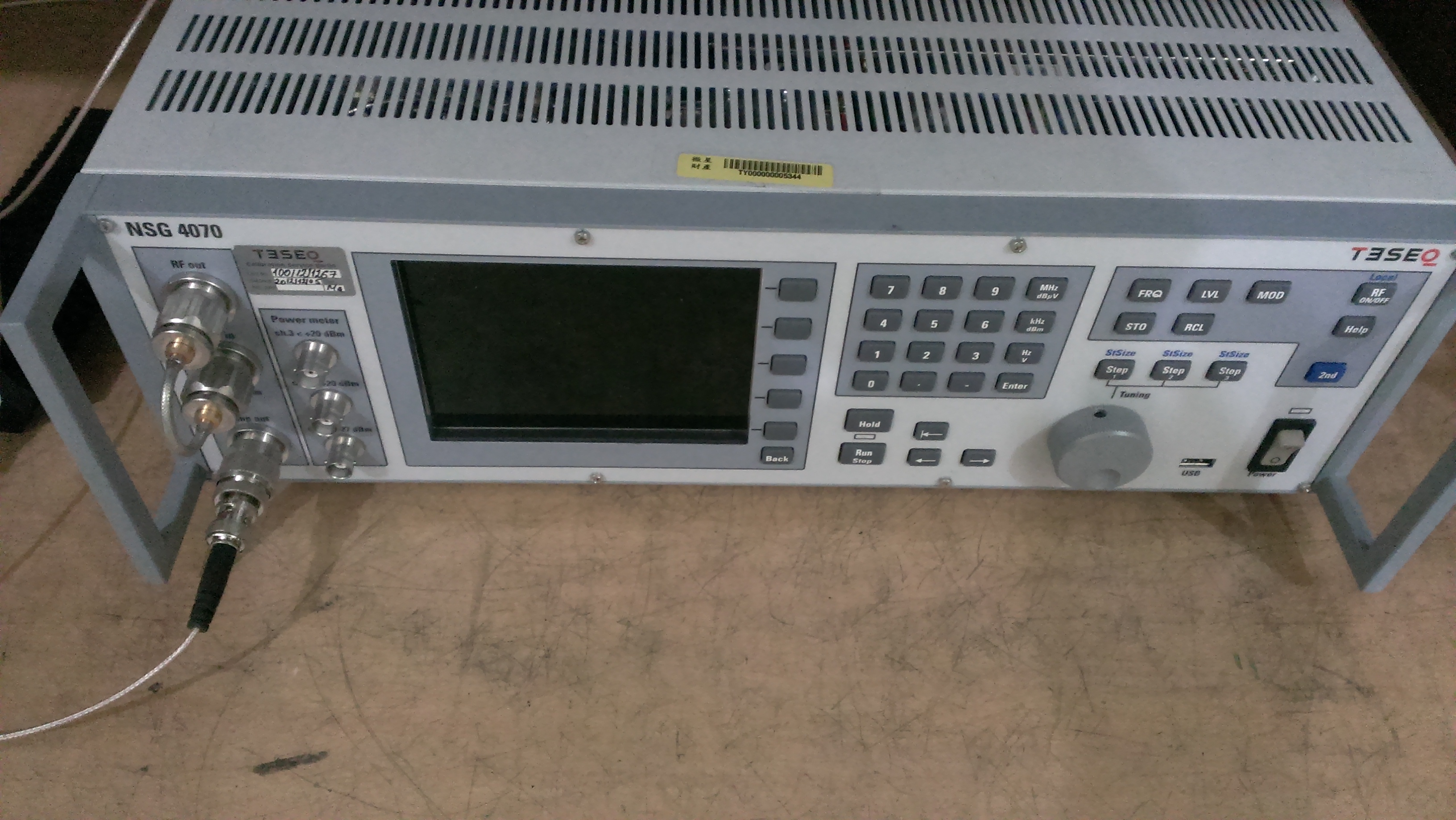
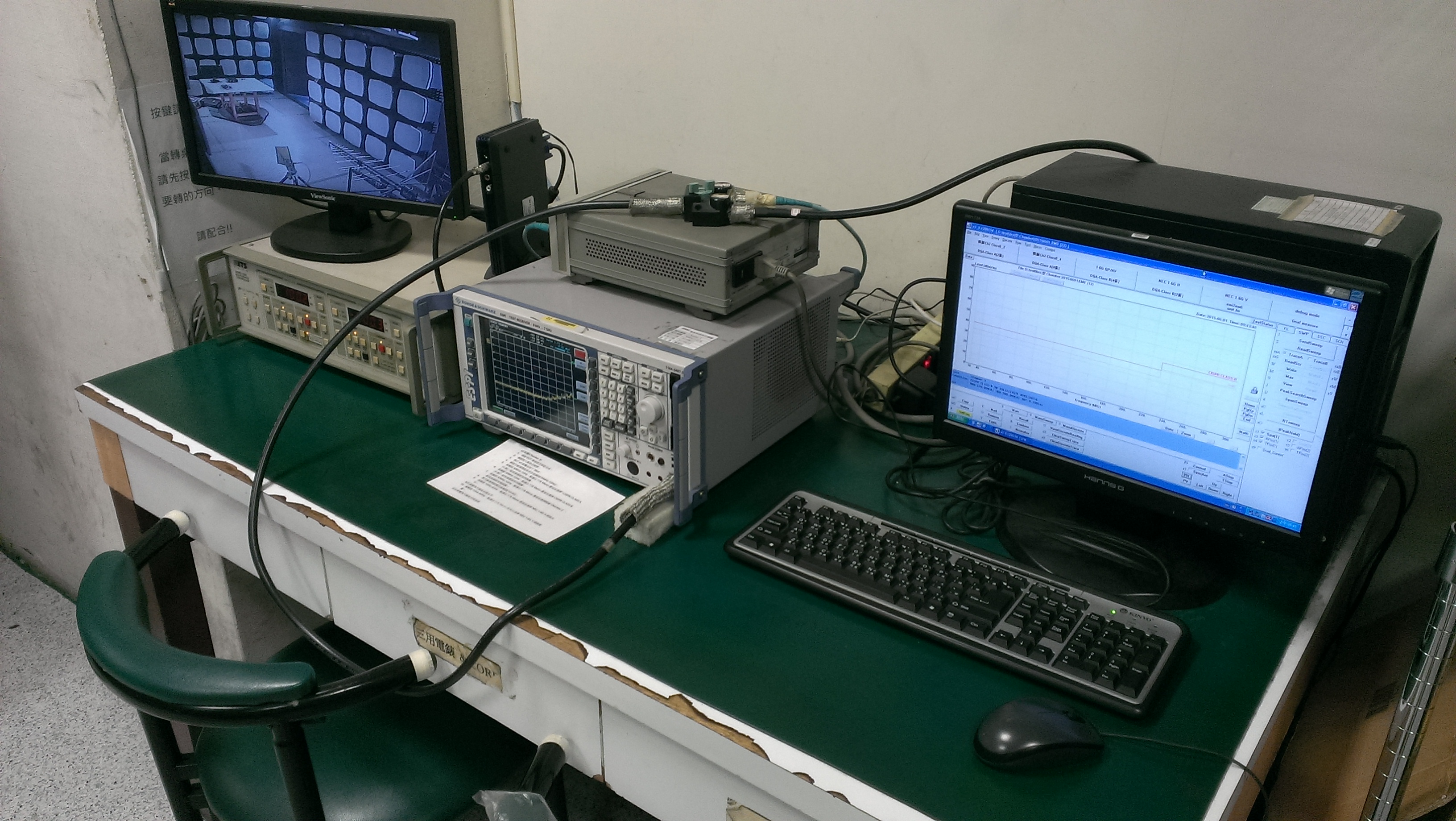
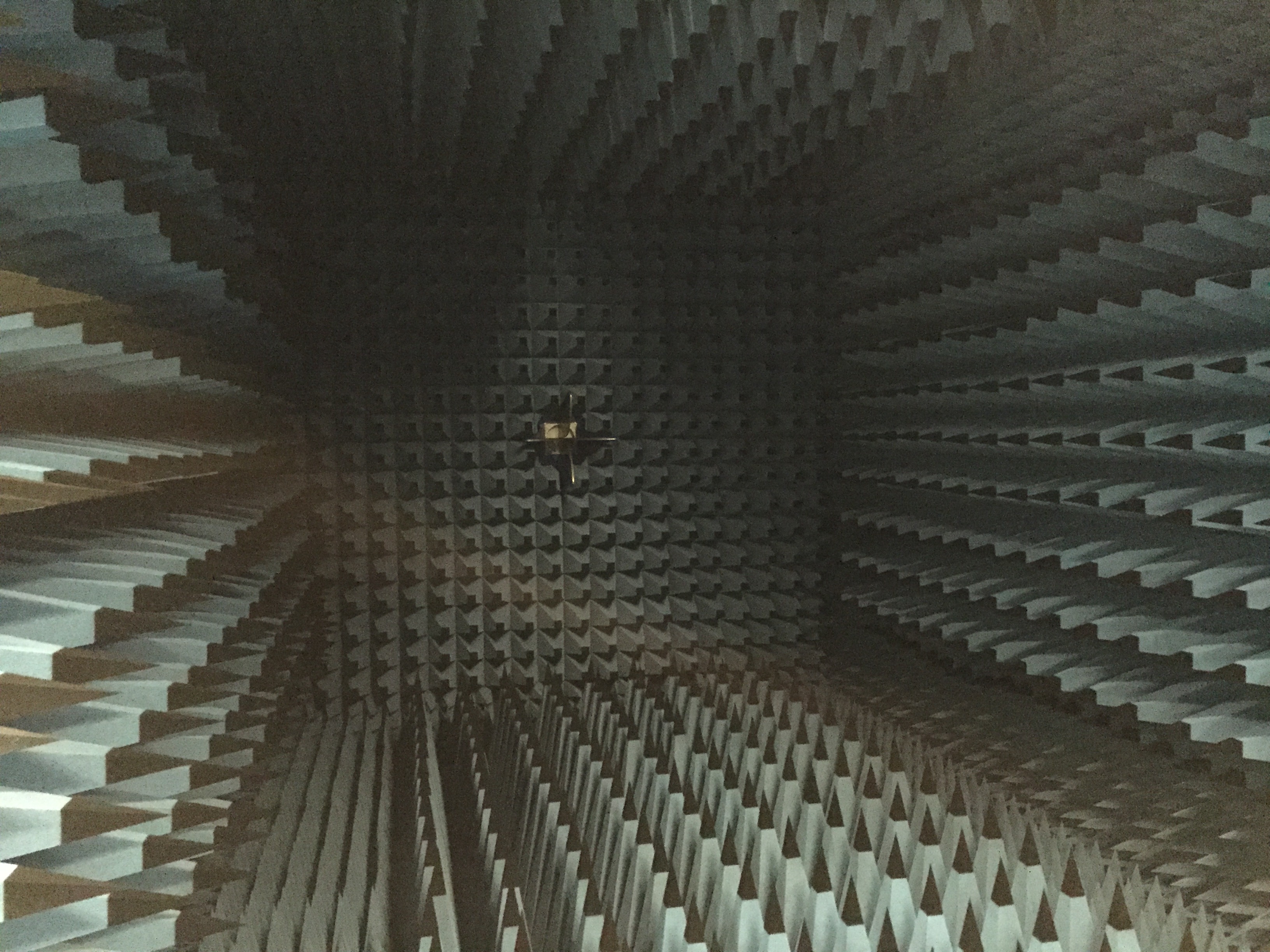
A lot of the facilities I was shown around involve extensive RF testing, both in terms of audible noise and adhering to individual standards. Previously in other HQ Tours I tend to be shown one room (specifically the semi-anechoic chamber which is really fun to be in), but here we had a combination of those as well as various microwave/other-RF facilities due to MSI’s extensive wireless portfolio of products.
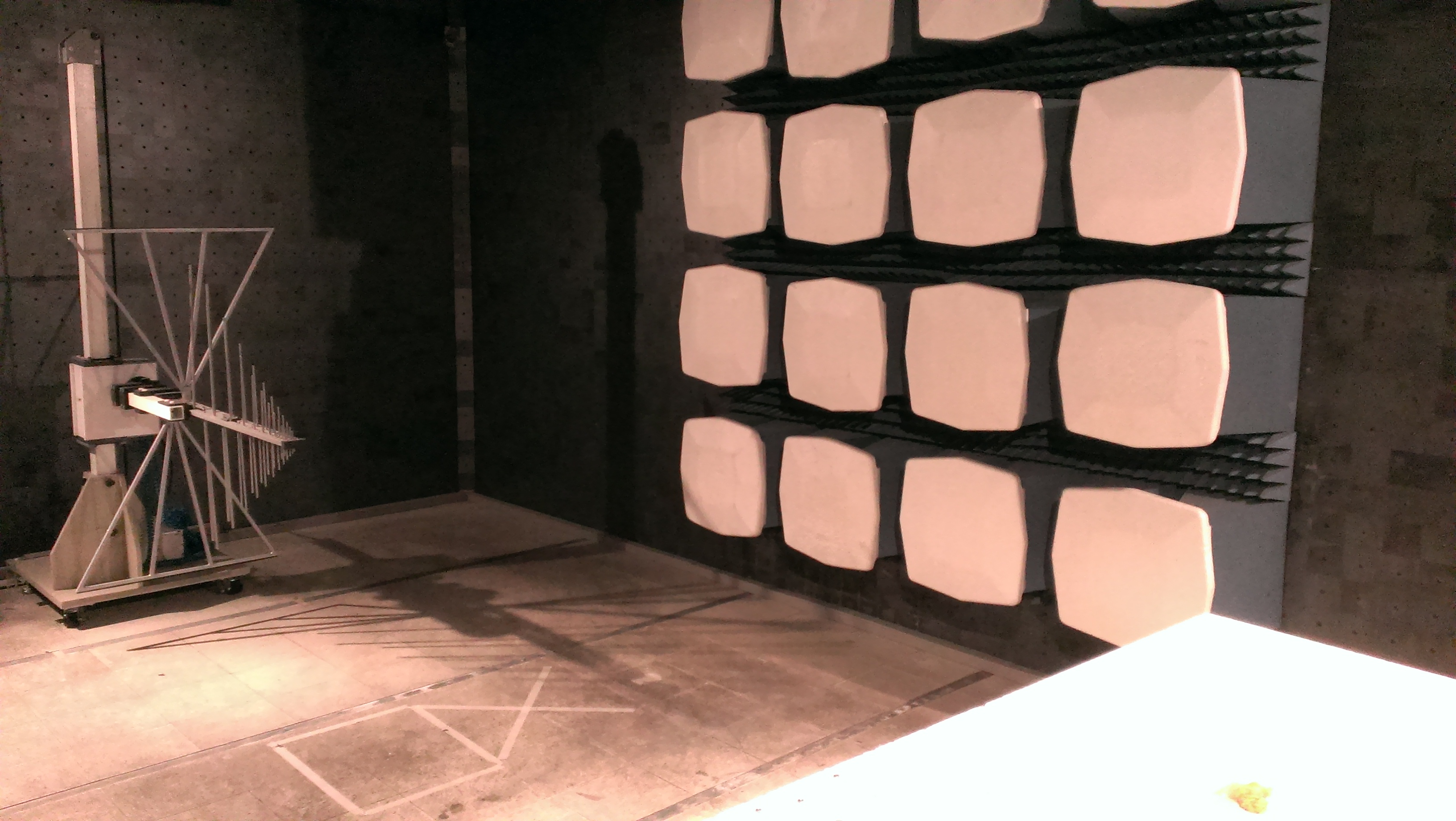
Again, this stems from MSI’s Military Class angle of marketing, and as such each design has to be tested before it moves off to be verified. Each one of these rooms can easily cost around 6-figures, including the construction of the room and the specific equipment needed:

I should note here that MSI did not show me around any of the drop-test or vibration facilities which I’ve seen in other places. In fact, these testing rooms above were located either above the fourth floor or down in the basement, whereas in two other HQ Tours they have all been in the basement.
Perhaps something new that I hadn’t seen before is spark testing.
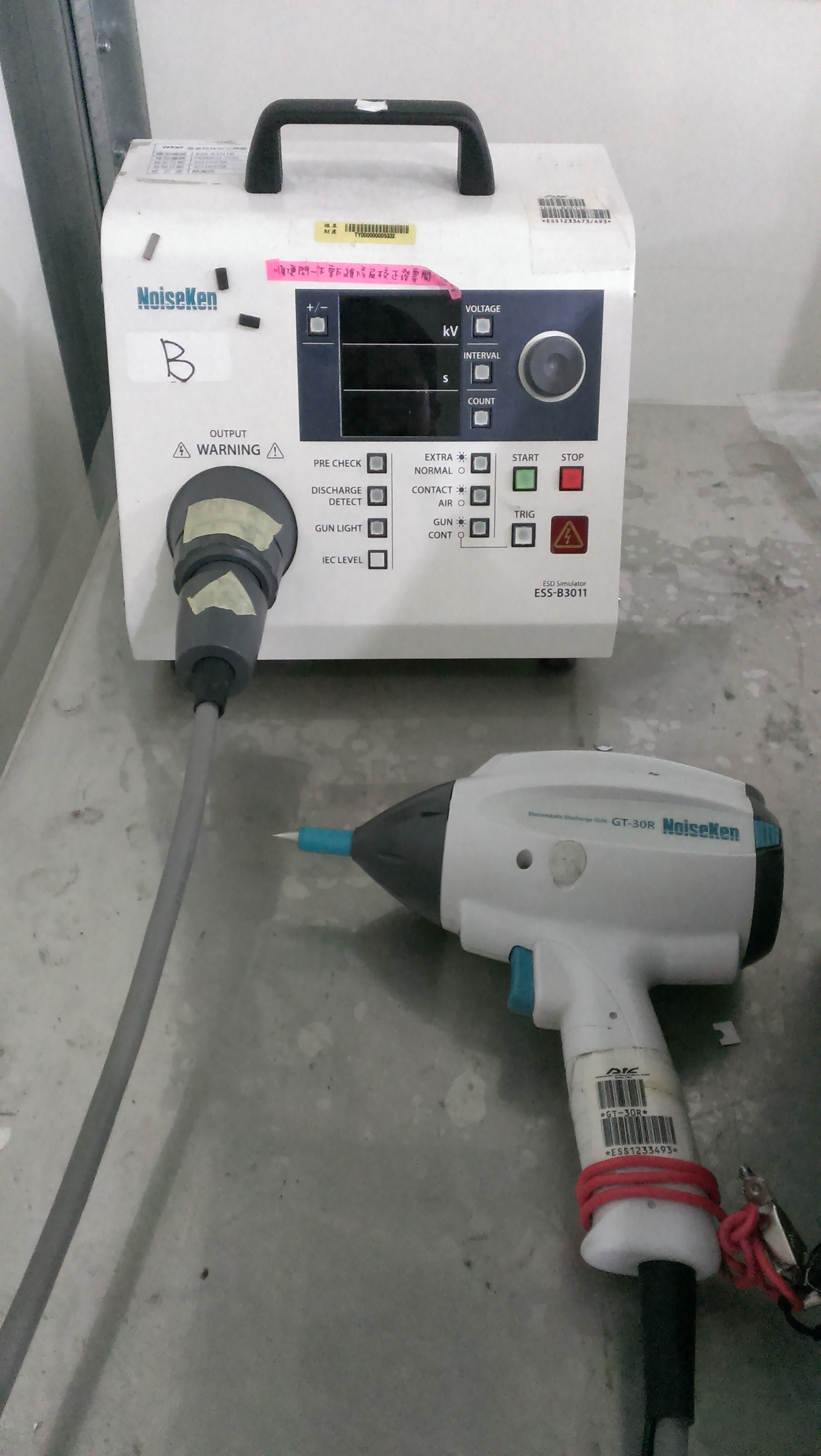
As it was explained to me, this device can generate a 12 kV differential and they use it to check that components on the product are adequately shielded from intense sparking.


23 Comments
View All Comments
willis936 - Wednesday, July 8, 2015 - link
How do you get the job of overclocking for a living? Do you need 20 years of firmware design experience or what?Ian Cutress - Thursday, July 9, 2015 - link
Typically most of the top 10 in the world are affiliated with a manufacturer, so if you can make a dent there, you can get on the radar. Having detailed knowledge of power delivery systems and how to manipulate those also helps. It's basically EE for the purpose of all-out performance. But very few actually make that step from hobby to professional. Most professionals work with motherboard design teams rather than competing in contests these days. Some work for retailers (8Pack) and they're used as a marketing tool for pre-built systems and such.Lotos - Monday, July 27, 2015 - link
Many of these tests come from the Aerospace document DO-160, I wouldn't be surprised if that is what MSI tests to. The last test denoted as a "spark" test is actually a ESD test. They'll charge the devices/components up to a certain voltage and make sure that the device is not susceptible to the high levels of static and to ensure that the device adequately drains the charge without harming itself.